728x90

728x90

Showing posts with label PIC18F4550. Show all posts

Tuesday, August 2, 2022

PIC18F4550 Programming Using MPLabX

PIC18F4550 is an enhanced Flash micro-controller with USB 2.0 feature. This device can operate up to 48MHz that yield the executing speed up to 12MIPS.

PIC18F4550 Programming in MPLabX
PIC18F4550 Family Data Summary

PIC18F4550 Programming in MPLabX

Program testing on target board

 There are some compilers available to program this device,

  • MPLABX XC8
  • MikroC Pro for PIC
  • IAR for PIC18
  • CCS PICC, and etc.

MPLABX XC8 is a free compiler from this device manufacturer. We can buy a paid version for a higher code generation quality.

In this example I use the MPLABX IDE to get start with this device programming. I use the latest version of MPLABX of 6.0, and the XC8 compiler of 2.40.

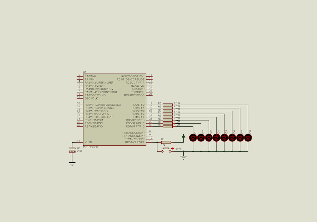
The program will chase the output LED(s) connect to PORTD.

PIC18F4550 Programming in MPLabX
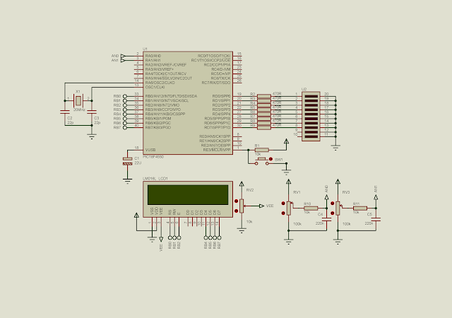
Schematic
Source Code:

  1. /*
  2.  * File: main.c
  3.  * Author: aki-technical
  4.  *
  5.  * Created on August 1, 2022, 6:22 PM
  6.  */
  7.  
  8. #include <xc.h>
  9. #include "config18f4550.h"
  10.  
  11. #define _XTAL_FREQ 20000000
  12.  
  13. void main(void) {
  14. PORTD=0x00;
  15. LATD=0x00;
  16. TRISD=0x00;
  17. LATD=0x01;
  18. while(1){
  19. LATD=0x01;
  20. while(LATD!=0){
  21. LATD<<=1;
  22. __delay_ms(50);
  23. }
  24. }
  25. return;
  26. }
  27.  

Configuration File:

  1. // CONFIG1L
  2. #pragma config PLLDIV = 1
  3. #pragma config CPUDIV = OSC1_PLL2
  4. #pragma config USBDIV = 1
  5.  
  6. // CONFIG1H
  7. #pragma config FOSC = HS
  8. #pragma config FCMEN = OFF
  9. #pragma config IESO = OFF
  10. // CONFIG2L
  11. #pragma config PWRT = OFF
  12. #pragma config BOR = OFF
  13. #pragma config BORV = 3
  14. #pragma config VREGEN = OFF
  15.  
  16. // CONFIG2H
  17. #pragma config WDT = OFF
  18. #pragma config WDTPS = 32768
  19.  
  20. // CONFIG3H
  21. #pragma config CCP2MX = OFF
  22. #pragma config PBADEN = OFF
  23. #pragma config LPT1OSC = OFF
  24. #pragma config MCLRE = ON
  25.  
  26. // CONFIG4L
  27. #pragma config STVREN = OFF
  28. #pragma config LVP = OFF
  29. #pragma config ICPRT = OFF
  30. #pragma config XINST = OFF
  31.  
  32. // CONFIG5L
  33. #pragma config CP0 = OFF
  34. #pragma config CP1 = OFF
  35. #pragma config CP2 = OFF
  36. #pragma config CP3 = OFF
  37.  
  38. // CONFIG5H
  39. #pragma config CPB = OFF
  40. #pragma config CPD = OFF
  41.  
  42. // CONFIG6L
  43. #pragma config WRT0 = OFF
  44. #pragma config WRT1 = OFF
  45. #pragma config WRT2 = OFF
  46. #pragma config WRT3 = OFF
  47.  
  48. // CONFIG6H
  49. #pragma config WRTC = OFF
  50. #pragma config WRTB = OFF
  51. #pragma config WRTD = OFF
  52.  
  53. // CONFIG7L
  54. #pragma config EBTR0 = OFF
  55. #pragma config EBTR1 = OFF
  56. #pragma config EBTR2 = OFF
  57. #pragma config EBTR3 = OFF
  58.  
  59. // CONFIG7H
  60. #pragma config EBTRB = OFF
  61.  

Click here to download its source file. I use Protues 8.10 SP3 to simulate this program. Now let try an random LED output on PORTD.

  1. /*
  2.  * File: main.c
  3.  * Author: aki-technical
  4.  *
  5.  * Created on August 1, 2022, 6:22 PM
  6.  */
  7.  
  8. #include <xc.h>
  9. #include "config18f4550.h"
  10.  
  11. #define _XTAL_FREQ 20000000
  12.  
  13. void main(void) {
  14. PORTD=0x00;
  15. LATD=0x00;
  16. TRISD=0x00;
  17. LATD=0x01;
  18. while(1){
  19. LATD=rand();
  20. __delay_ms(50);
  21. }
  22. return;
  23. }
  24.  

The schematic diagram remains the same as the previous one's.

Wednesday, March 3, 2021

Making a PIC18F4550 Learning Board

Overview

PIC18F4550 is an 8-bit micro-controller from Microchip. In the PIC18 series, it has a built-in USB communication module inside. In prototyping we usually built the circuit on a bread board with some jumper wire. It usually cause damage to the device when we wrongly connect the circuit.

making a PIC18F4550 Learning Board
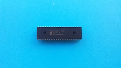
PIC18F4550 in DIP package I posses. 

Using a per-soldered board most of prototyping is safer and more reliable. Some ready made learning board could be found on E bay or  Amazon below 10 US Dollars.

PCB Project Design And Make

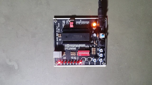
However, we can build our own learning board at home using a dozen of existing components. I made a simple learning board by myself at free time. The design fits any 40-pin 8-bit PIC device. But I tend to use PIC18F4550 with a USB type-B connector on board.
 
making a PIC18F4550 Learning Board
A Completed Assembling
 

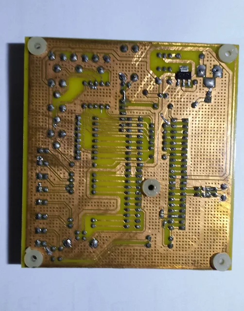
making a PIC18F4550 Learning Board
Bottom side

These are some building block of the board:
  1. A +12 V to +5 V DC regulated power supply
  2. A soldered crystal clock and reset circuit
  3. A 6-pin ICSP connector for downloading the program
  4. A USB type-B connector
  5. A DIP switch connected to PORTB
  6. An 8-bit LED connected to PORTD
  7. Six POTs  connected to analog input pins RA0 to RA5
I have already test the functionalities of this board and it's fully worked.

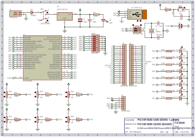
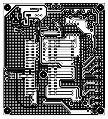
The overall schematic and PCB design are made using Proteus 8.

making a PIC18F4550 Learning Board
Schematic Diagram


making a PIC18F4550 Learning Board
Copper Side

making a PIC18F4550 Learning Board
Components Side
 

PIC18F4550 Tutorials In CCS PICC

Wednesday, February 17, 2021

Start To Blink PIC18F4550 Using CCS PICC

Overview Of PIC18F4550

PIC18F4550 is an 8-bit PICMicro built with a USB peripheral inside.  It could clock up to 48 MHz to full fill its USB hardware requirements. The program memory size is 16384 words. It temporary memory SRAM is 2048 KB with an auxiliary non-volatile memory of 256 Bytes.

By selecting its 40-pin DIP package, the digital I/O ports available up to five ports with 35 usable inputs outputs. 

A stable direct current voltage source powers this device between 2 V and 5.5 V, depends on the operating frequency. The higher clock frequency requires a higher supply voltage. Typically, a hobbyist prototyping require a 5 V supply voltage.

PIC18F4550-I/P I stock and its pin diagram

There are five 8-bit ports list from PORTA to PORTD. They are,
  1. PORTA
  2. PORTB
  3. PORTC
  4. PORTD
  5. and PORTE.
All ports are programmable bi-directional I/O. Any ports has other special functions other than the digital I/O.

Interfacing And Programming

I select my DIY PIC18F4550 board I made to work with this example. On this board PORTD connects to an 8-bit LED output.
CCS PICC compiler has a lot of library functions. For digital input output, we need to use a few functions.
  1. output_x(value) - Writes an 8-bit data to any port x ( eg, A, B, C, etc).
  2. set_tris_x(value) - Set the data direction of x port. The value of 0 means output direction, otherwise an input direction.
  3. delay_ms(time) - Creates a timing delay in milli seconds. Time is an unsigned 16-bit integer ( 0 to 65535) milli seconds.
To program in CCS PICC:
  • include the device header file
  • use 'fuses' directive to set the configuration bits
  • use 'delay' directive to set the clock of the CPU
  • write the main function and others.

CCS PICC Source Code From GitHub


Schematic Diagram


Start To Blink PIC18F4550 Using CCS PICC
Schematic Diagram

Click here to download this example in zip file.


Monday, February 15, 2021

PIC18F4550 Basic ADC Programming In CCS PICC

Introduction To ADC Module Of PIC18F4550


PIC18F4550 has a 10-bit ADC module. There are 13 analog input channels within PORTA and PORTB.


These analog input pins are multiplexed with digital input pins. By default, they are analog input pins.


Voltage Reference

There two analog voltage reference pins - VREF+ (RA3) and VREF-(RA2). these two pins are optional. 


They could be wired to external voltage reference source, or internally wired to VDD and GND, by software default setting. However, the total reference voltage must not exceed 5 V DC in magnitude.


Clock Source

Clock source fed to the ADC module come from its internal ADC RC oscillator, or the MCU clock source with programmable prescaler, up to 1:64.


Interfacing And Programming


Unlike writing a program in a low level language like assembly language, using a high level C programming language could make it done in a short time. CCS PICC provide a lot of peripherals libraries for those PICMicro devices including the PIC18F4550.


Those programmings in assembly need to know about the technical details of the module, especially the registers setting the make the peripheral to operate properly. However in a high level C for embedded controllers, those technical details were summarized in a few C syntax of its function library.


CCS PICC ADC Functional Overview

All functions list below make a configuration and the operation of the ADC module.

  1. setup_adc(mode) - select adc mode like on/off, adc clock etc.
  2. setup_adc_port(value) - set the number of available pins on the targeting device. The reference voltage pins could be include here.
  3. set_adc_channel(channel) - select the specific channel to convert.
  4. read_adc(mode) - start the conversion and return the result
  5. adc_done() - it's useful for testing the result. It return 0 if the conversion is completed.

By default the ADC result is 8-bit wide even the device's ADC is 10-bit. To use the device's full 10-bit resolution, use the #DEVICE ADC=10 after the device header file declaration.

Interfacing And Programming

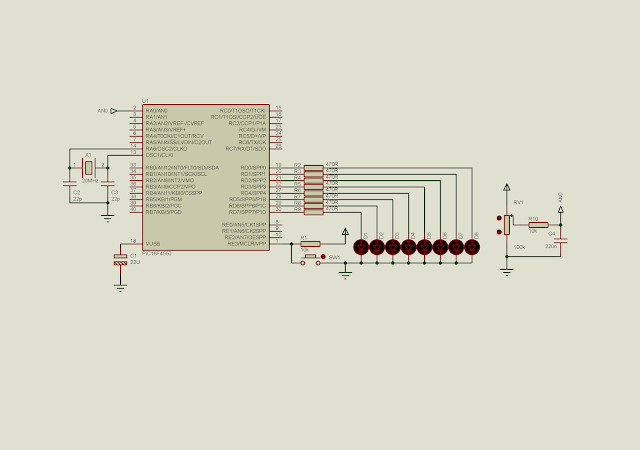
AN0 is the ADC channel 0 locates at RA0 of PORTA. This analog input channel read an analog input voltage value up to +5 V DC. The result is by default 8-bit. This 8-bit result display at the 8-bit PORTD output.
I configure the ADC clock to fed from its internal RC oscillator. Voltage reference for the ADC is internally wired to VDD and GND. MCU supplies at + 5 V DC. An external crystal is a 20 MHz crystal oscillator. 

PIC18F4550 Basic ADC Programming In CCS PICC
Schematic Diagram

Source stored in GitHub gist.

Click here to download archive of this example.

PIC18F4550 Basic ADC Programming In CCS PICC
A running program


LED Bar Graph Voltage Level Indicator With PIC18F4550

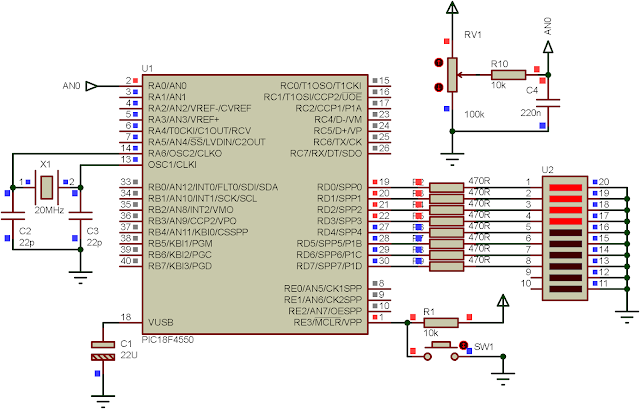
In the previous post, we show how to use ADC library function in CCS PICC. Here, the ADC is still in the discussion. In this example, I use almost the same source code, but one's difference is the output LED displays a bar graph pattern indicating the level of input voltage reading from the AN0.


ADC result is still 8-bit. This 8-bit result is scaled into an 9 number values correspond to 8 output LEDs on PORTD.


LED Bar Graph Voltage Level Indicator With PIC18F4550
LED bar graph running

Source code from GitHub gist.


Click here to download this example in zip file.

Schematic Diagram


Saturday, January 2, 2021

PIC18F4550 LCD Interfacing in CCS PICC

A character LCD traditional built with a controller inside especially the HD44780. It's easy to control with some basic LCD instruction. For more technical details and programming interface for this type of LCD controller click here to view. Character LCD are available from as single to multiple lines and multiple characters.


PIC18F4550 Interfaces To Character LCD
A running Program

In CCS PIC an LCD software driver is ready to use in side the compiler. The LCD.C driver could control a character LCD only for two line character LCD. Within this driver there are a lot of functions lists below.

  1. lcd_init() - must be called before calling other function
  2. lcd_putc() - send one character to LCD
  3. lcd_gotoxy(x,y) - set write position on LCD, start from 1,1
  4. lcd_getc(x,y) - return character at the position x,y on  LCD
  5. lcd_cursor_on(int1 on) - turn on cursor
  6. lcd_set_cgram_char(w,*p) - write custom character to CGRAM
In this example, the LCD prints the duration of MCU started up time. The C printf function could be use to send the character to LCD by adding the LCD_PUTC stream to this function.


Click here to download this example in zip file.

PIC18F4550 Interfaces To Character LCD
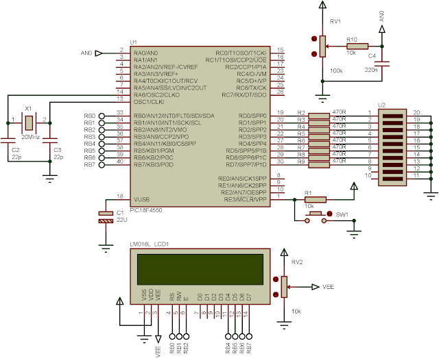
Schematic Diagram


ADC vs Analog Voltage Displaying with PIC18F4550 in CCS PICC

In previous posts, I have shown about using the ADC module of PIC18F4550 programming, and LCD programming interface in CCS PICC

In this post, I use PIC18F4550 to read two analog input channels. A character LCD as used in the previous post displays the value of ADC reading of each channel and its analog voltage value. However, here I use the full 10-bit ADC resolution of this device.

PIC18F4550 ADC Reading And LCD Displaying With CCS PICC
ADC reading and its value displaying

Source code from GitHub gist:

Click here to download zip file of this example.

PIC18F4550 ADC Reading And LCD Displaying With CCS PICC
Schematic Diagram


LM35 and LCD Temperature Displaying with PIC18F4550 in CCS PICC

Referring to ADC module of PIC18F4550, there are many analog output sensor to interfaces with this MCU. LM35 is a simple analog temperature sensor, creating analog voltage output representing its temperature conversion in degree Celsius. The step temperature from this device is 10 mV per degree Celsius. I don't want to put all its details here. For more information about using this device, please see this post.


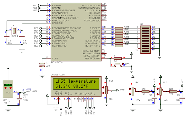
In this post, LM35 connects to AN2 analog channel of the ADC. The MCU reads the analog voltage, converting it to temperature value in both degree Celsius and degree Fahrenheit.


PIC18F4550 interfaces to LM35 and LCD
A temperature reading of 31.2 degree Celsius.

A very simple LM35 comes in a transistor-like TO-92 package.

LM35DZ in TO-92 package.

C source code fed from GitHub.


Click here to download the zip file of this example.

PIC18F4550 interfaces to LM35 and LCD
Schematic Diagram


PIC18F4550 PWM Example in CCS PICC

Overview

Creating a varied analog voltage output from an MCU require an analog voltage generator, PWM (pulse width modulation). Making a analog voltage PWM to work, the user needs to know about all relevant register configurations to set the frequency and duty cycle of PWM signal.

However, in a high level embedded language, creating a PWM signal output doesn't need a deep level of low level hardware/register configuration. With a few C functions, the PWM signal output from any MCU could be created in a few minutes.

CCS PICC Basic Pulse Width Modulation Programming

Without using any technical detail of PWM software setting, we can create a PWM output from scratch with this compiler. In this introductory example, I use only a few C code to program the PWM.

  1. #use PWM directive
  2. pwm_set_duty_percent()
The directive #use PWM has many options, but I list a few commonly use options of this.
  • CCPx or PWMx - Select a CCP/PWM module
  • FREQUENCY=x - Set the frequency of PWM signal
  • PERIOD=x - Set the period of PWM signal
  • DUTY=x - The default duty cycle is 50% if it's not set.
For more details about this directive, check the compiler manual.

The pwm_set_duty_percent specifies the duty cycle of PWM output signal. The syntax is pwm_set_duty_percent(stream,value). Where stream is optional, and value is ranges from 0 to 1000. For example when value = 500, the PWM duty cycle is 50% and so on.

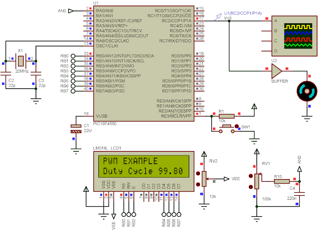
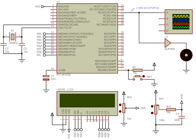
In this introductory example, I set a fixed frequency of PWM and a variable duty cycle. Duty cycle is adjusted by the variation of a POT. CCP1 is selected to make the PWM signal.

CCS PICC basic PWM example with PIC18F4550
I adjust the POT to the MAX.

C Source Code


Schematic 

CCS PICC basic PWM example with PIC18F4550
Schematic Diagram

Click here to download this example in zip file.

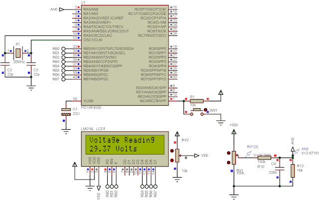
PIC18F4550 ADC Simple Digital Volt Meter

The ADC module of PIC18F4550 could read an analog input voltage up to 5 V DC with some DC offset. However, the outside analog voltage fed to the ADC could be greater than 5 V DC by adding a simple voltage divider circuit. 

The voltage divider circuit is very simple, built by two resistors in this case. The output voltage from the divider circuit is smaller than the input according to the dividing factor. The factor created by picking up a different resistances of the selected's. The designer may decide and take a little math calculation using voltage divider theorem to get a specific division factor. 

I don't show the overall process of math calculation here. You can see this post to get a full detail.

A simple DIY DC voltmeter with PIC18F4550
The MCU reads the analog input voltage fed to RA0.

PICC Source Code


Schematic Diagram

A simple DIY DC voltmeter with PIC18F4550
Schematic Diagram

Click here to download the zip file of this example.

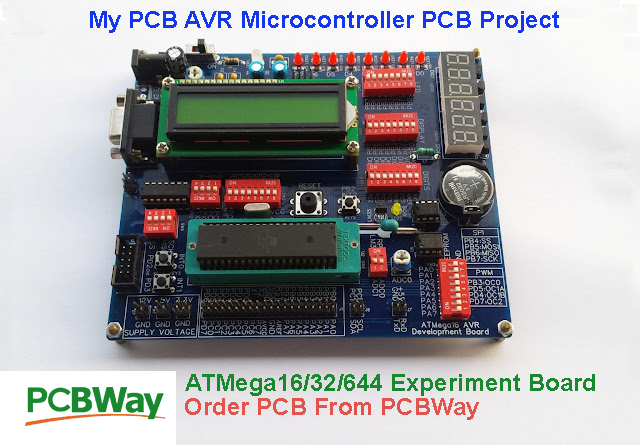
If you want a standard PCB for ATMega32 micro-controller, you can order my AVR Microcontroller project from PCBWay with a reasonable price. Click here to get a free $5 credit for new account.

Interfacing ATMega32 to 74HC595 shift register
ATMega16 ATMega32 Experiment Board PCB from PCBWay


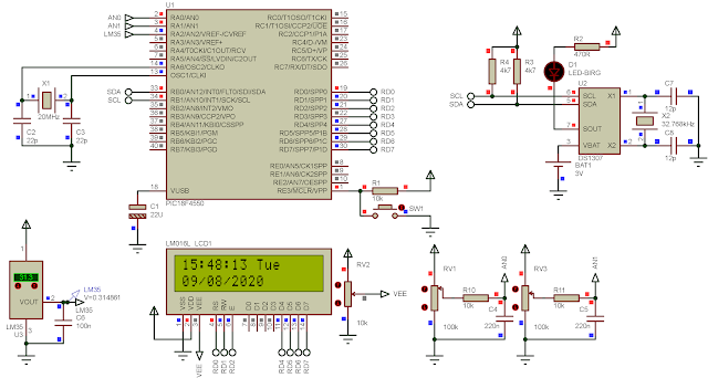
PIC18F4550 DS1307 I2C RTC LCD Interfacing

PIC18F4550 has a master synchronous serial ports (MSSP) module inside. This module consist of two sub-communication modules - I2C and SPI. An I2C is communication protocol for short range, low data rate requires only two pins - Serial Data(SDA) and Serial Clock(SCL). However, the SPI communication port doesn't lists here.


DS1307 is a real time clock keeper with I2C communication interface. This device keep the time running by an external crystal clock of 32.768 kHz. Even the supply voltage is off, a coin back up battery keep the data RAM synchronizes for future use. Since an I2C is use for communication, there are two communication pins - SDA and SCL. These two pins are open drain, require an individual external pull up resistor. The resistor ranges from 4.7 kOhm to 10 kOhm resistance.


For more technical details about DS1307, please see this post on another blog I wrote.


In this programming example, PIC18F4550 uses its I2C master to write and read timing data from DS1307 I2C slave device. Those data will display on a character display.


PIC18F4550 interfaces to DS1307 RTC and character LCD
Circuit Simulation

PICC Source Code

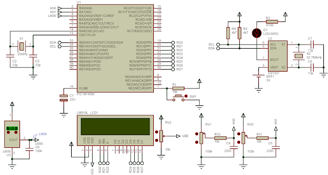
Schematic Diagram

PIC18F4550 interfaces to DS1307 RTC and character LCD
Schematic Diagram

Click here to download the zip file of this example.


Tuesday, December 22, 2020

Interfacing PIC18F4550 to 74HC595 CCS PICC

A shift register chip is very useful for expanding the digital I/O. Getting more digital outputs, the 74HC595 is very popular due to its ease of use. It is called a serial in parallel out shift register IC. The 74XX prefix belong to the clue logic family of the digital IC.

74HC595 chips in DIP package

The communication interface between the MCU and this controller is quite simple. It basically use three pins as in the form of the Serial Peripheral Interface (SPI) which are,

  • Serial Data
  • Serial Clock
  • Enable

This IC has an 8 bit output with an optional serial data out for a daisy-chain connection.

Pin diagram of this device

An SPI communication that used by the MCU to send the data to this chip could be an SPI peripheral inside the MCU, or a software bit-banging written by the programmer. The SPI peripheral usually has a fixed pins but using the software bit-banging the output pins are select-able by the programmer.

With the software bit-banging, the program need to spend more more time executing this SPI-like communication. In this case it doesn't provide a high speed SPI.

CCS PICC has a built-in driver allowing the PIC microcontroller to send a serial data to this chip. We need to set up some basic steps as shown below:

  1. Select a serial data pin
  2. Select a serial clock pin
  3. Select a enable pin
  4. Set the numbers of register
  5. Send some bytes of data with a preset numbers of register

The 74595.c is ready to use in the CCS PICC compiler after the installation. The write_expanded_outputs(eo) function writes some bytes to this chip. The number of bytes is a preset number of register.

In this example, PIC18F4550 connects to a two-digit display driven by two distinct shift registers. The MCU counts the number of input up to 99 before it reset to 0.

PIC18F4550 Interfaces To 74HC595 Shift Registers
Schematic Diagram

Source of this program is written using CCS PICC.

#include<18f4550.h>

/*Use high speed clock no PLL prescaler 
no system clock post scaler */
#fuses HS,PLL1,CPUDIV1,NOWDT
#use delay(clock=20M)

#define EXP_OUT_ENABLE  PIN_D0
#define EXP_OUT_CLOCK   PIN_D1
#define EXP_OUT_DO      PIN_D2
#define NUMBER_OF_74595 2

#include<74595.c>


void main(void){
unsigned char patterns[16]={0x3F,0x06,0x5B,0x4F,0x66,0x6D,0x7D,
 0x07,0x7F,0x6F,0x77,0x7C,0x39,0x5E,0x79,0x71};
   unsigned char cnt=0;
   unsigned char digits[2];
   //Clear PORTD
   output_D(0x00);
   //Set PORTD To Output
   set_tris_D(0x00);
   
      
   while(1){
      digits[0]=patterns[cnt/10];
      digits[1]=patterns[cnt%10];
      write_expanded_outputs(&digits);
      delay_ms(1000);
      cnt++;
      if(cnt>=100) cnt=0;
   }
}


320x50

Search This Blog

Labels

25AA010A (1) 8051 (7) 93AA46B (1) ADC (30) Analog Comparator (1) Arduino (15) ARM (6) AT89C52 (7) ATMega32 (57) AVR (58) CCS PICC (28) DAC (1) DHT11 (2) Display (106) Distance Sensor (3) DS18B20 (3) dsPIC (3) dsPIC30F1010 (3) dsPIC30F2010 (1) EEPROM (5) Environment Sensor (4) esp8266 (1) I2C (29) Input/Output (68) Interrupt (19) Keil (5) Keypad (10) LCD (48) Master/Slave (1) MAX7221 (1) MCP23017 (5) MCP23S17 (4) Meter (3) MikroC (2) Motor (15) MPLABX (73) Nokia 5110 LCD (3) OLED (2) One-Wire (6) Oscillator (8) PCB (10) PCD8544 (3) PCF8574 (5) PIC (108) PIC12F (3) PIC16F628A (3) PIC16F630 (2) PIC16F716 (4) PIC16F818 (11) PIC16F818/819 (3) PIC16F84A (16) PIC16F876A (2) PIC16F877A (9) PIC16F88 (2) PIC16F887 (60) PIC18 (19) PIC18F1220 (5) PIC18F2550 (5) PIC18F4550 (12) PICKit2 (1) PWM (11) RTC (9) Sensor (11) SH1106 (1) Shift Register (11) Shift Registers (3) SPI (24) STM32 (6) STM32 Blue Pill (6) STM32CubeIDE (6) STM32F103C8T6 (6) SysTick (3) temperature sensor (11) Thermometer (21) Timer/Counter (31) TM1637 (2) UART (7) Ultrasonic (4) Voltmeter (7) WDT (1) XC16 (2) XC8 (96)

tyro-728x90