Overview
The Microchip Technology Inc. 23X256 is a 256-Kbit Serial SRAM device. The memory is accessed via a simple Serial Peripheral Interface (SPI) compatible serial bus. The bus signals required are a clock input (SCK) plus separate data in (SI) and data out (SO) lines. Access to the device is controlled through a Chip Select (CS) input. Communication to the device can be paused via the hold pin (HOLD). While the device is paused, transitions on its inputs will be ignored, with the exception of Chip Select, allowing the host to service higher priority interrupts.
It supports clock rate up to 10MHz via its SPI interface. There many write and read modes, byte mode, page mode and sequential mode. Each pages contains 32 bytes of data.

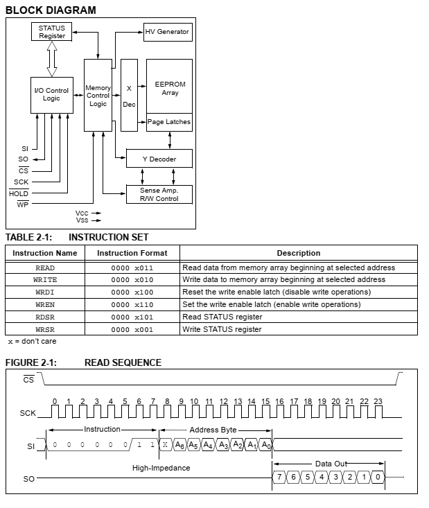
This SPI chip does not have an address but it has some command before able read and write to this chip. Command or instruction locate at the first byte of data transmission. For example 0x03 for READ and 0x02 for WRITE.
 |
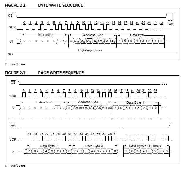
| Data read and write using byte mode |
By default this device operates in byte read or write mode.
ATMega644P and 23K256 Interfacing
To get start the master ATMega644P MCU write and read data from this chip using byte mode. SRAM data will display on PORTC.
 |
| Schematic |
Source Code "main.c":
- /*
- * 12-spi_23K256.c
- *
- * Created: 2/25/2026 9:31:10 AM
- * Author : Admin
- */
- #include <avr/io.h>
- #include <util/delay.h>
- #define F_CPU 16000000UL
- #define DDR_SPI DDRB
- #define PRT_SPI PORTB
- #define DD_SS 4
- #define DD_MOSI 5
- #define DD_MISO 6
- #define DD_SCK 7
- void SPI_MasterInit(void)
- {
- /* Set MOSI and SCK output, all others input */
- DDR_SPI = (1<<DD_MOSI)|(1<<DD_SCK)|(1<<DD_SS);
- /* Enable SPI, Master, set clock rate fck/16 */
- SPCR = (1<<SPE)|(1<<MSTR)|(1<<SPR0);
- }
- void SPI_MasterTransmit(char cData)
- {
- /* Start transmission */
- SPDR = cData;
- /* Wait for transmission complete */
- while(!(SPSR & (1<<SPIF)))
- ;
- }
- void SPI_SlaveInit(void)
- {
- /* Set MISO output, all others input */
- DDR_SPI = (1<<DD_MISO);
- /* Enable SPI */
- SPCR = (1<<SPE);
- }
- char SPI_SlaveReceive(void)
- {
- /* Wait for reception complete */
- while(!(SPSR & (1<<SPIF)))
- ;
- /* Return Data Register */
- return SPDR;
- }
- // 23K256 SPI SRAM
- void write_bytes_23K256(unsigned int address, unsigned char data){
- unsigned char temp;
- PRT_SPI&=~(1<<DD_SS);
- SPI_MasterTransmit(0x02);
- SPI_MasterTransmit(address>>8);
- SPI_MasterTransmit(address);
- SPI_MasterTransmit(data);
- PRT_SPI|=(1<<DD_SS);
- }
- unsigned char read_bytes_23K256(unsigned int address){
- PRT_SPI&=~(1<<DD_SS);
- SPI_MasterTransmit(0x03);
- SPI_MasterTransmit(address>>8);
- SPI_MasterTransmit(address);
- SPI_MasterTransmit(0xFF);
- unsigned char data=SPI_SlaveReceive();
- PRT_SPI|=(1<<DD_SS);
- return data;
- }
- int main(void)
- {
- /* Replace with your application code */
- SPI_MasterInit();
- PRT_SPI|=(1<<DD_SS);
- unsigned char temp=0, data[16];
- DDRC=0xFF;
- while (1)
- {
- for (unsigned int i=0;i<8;i++)
- {
- write_bytes_23K256(i,1<<i);
- PORTC=read_bytes_23K256(i);
- _delay_ms(1000);
- }
- }
- }
Now I put a character LCD to show data reading from the 23K256. This chip still operate in byte mode data read and write.
 |
| Schematic |
Source Code "main.c":
- /*
- * 23K256_1602.c
- *
- * Created: 2/25/2026 10:50:02 AM
- * Author : Admin
- */
- #include <avr/io.h>
- #include <util/delay.h>
- #define F_CPU 16000000UL
- #define DDR_SPI DDRB
- #define PRT_SPI PORTB
- #define DD_SS 4
- #define DD_MOSI 5
- #define DD_MISO 6
- #define DD_SCK 7
- void delay_1(unsigned int value){
- for (unsigned int i=0;i<value;i++)
- {
- }
- }
- void SPI_MasterInit(void)
- {
- /* Set MOSI and SCK output, all others input */
- DDR_SPI = (1<<DD_MOSI)|(1<<DD_SCK)|(1<<DD_SS);
- /* Enable SPI, Master, set clock rate fck/16 */
- SPCR = (1<<SPE)|(1<<MSTR)|(1<<SPR0);
- }
- void SPI_MasterTransmit(char cData)
- {
- /* Start transmission */
- SPDR = cData;
- /* Wait for transmission complete */
- while(!(SPSR & (1<<SPIF)))
- ;
- }
- void SPI_SlaveInit(void)
- {
- /* Set MISO output, all others input */
- DDR_SPI = (1<<DD_MISO);
- /* Enable SPI */
- SPCR = (1<<SPE);
- }
- char SPI_SlaveReceive(void)
- {
- /* Wait for reception complete */
- while(!(SPSR & (1<<SPIF)))
- ;
- /* Return Data Register */
- return SPDR;
- }
- // 23K256 SPI SRAM
- void write_bytes_23K256(unsigned int address, unsigned char data){
- unsigned char temp;
- PRT_SPI&=~(1<<DD_SS);
- SPI_MasterTransmit(0x02);
- SPI_MasterTransmit(address>>8);
- SPI_MasterTransmit(address);
- SPI_MasterTransmit(data);
- PRT_SPI|=(1<<DD_SS);
- //delay_1(1000);
- }
- unsigned char read_bytes_23K256(unsigned int address){
- PRT_SPI&=~(1<<DD_SS);
- SPI_MasterTransmit(0x03);
- SPI_MasterTransmit(address>>8);
- SPI_MasterTransmit(address);
- SPI_MasterTransmit(0xFF);
- //delay_1(1000);
- unsigned char data=SPI_SlaveReceive();
- PRT_SPI|=(1<<DD_SS);
- return data;
- }
- int main(void)
- {
- /* Replace with your application code */
- _delay_ms(50);
- SPI_MasterInit();
- PRT_SPI|=(1<<DD_SS);
- unsigned char temp=0, data[16];
- lcd_init();
- lcd_clear();
- lcd_text("ATMega644P SRAM");
- lcd_xy(1,2);
- lcd_text("Serial 23K256");
- _delay_ms(10000);
- lcd_clear();
- for (unsigned int i=0;i<10;i++)
- {
- write_bytes_23K256(i,'0'+i);
- }
- for (unsigned int i=0;i<10;i++)
- {
- lcd_data(read_bytes_23K256(i));
- }
- lcd_xy(1,2);
- for (unsigned int i=0;i<16;i++)
- {
- write_bytes_23K256(i+10,'A'+i);
- }
- for (unsigned int i=0;i<16;i++)
- {
- lcd_data(read_bytes_23K256(i+10));
- }
- while (1)
- {
- }
- }
The LCD drivers are not here you can download this project package in download section below. I tested it on my AVR ATMega644P prototype board. It works fine and fast. But the wires connection problem between the prototype board and the bread board often cause problems to data communication.

Using sequential writing and reading mode could save processing time. However the master MCU must put the 23K256 to operate in this mode by writing an instruction to this chip.
 |
| Read Status Register Instruction |
The schematic is shown in previous example. The LCD shows the result of data reading from SRAM.
Source Code "main.c":
- /*
- * 23K256_Sequential_1602.c
- *
- * Created: 2/25/2026 2:37:30 PM
- * Author : Admin
- */
- #include <avr/io.h>
- #include <util/delay.h>
- #define F_CPU 16000000UL
- #include <stdio.h>
- #define DDR_SPI DDRB
- #define PRT_SPI PORTB
- #define DD_SS 4
- #define DD_MOSI 5
- #define DD_MISO 6
- #define DD_SCK 7
- void delay_1(unsigned int value){
- for (unsigned int i=0;i<value;i++)
- {
- }
- }
- void SPI_MasterInit(void)
- {
- /* Set MOSI and SCK output, all others input */
- DDR_SPI = (1<<DD_MOSI)|(1<<DD_SCK)|(1<<DD_SS);
- /* Enable SPI, Master, set clock rate fck/16 */
- SPCR = (1<<SPE)|(1<<MSTR)|(1<<SPR0);
- }
- void SPI_MasterTransmit(char cData)
- {
- /* Start transmission */
- SPDR = cData;
- /* Wait for transmission complete */
- while(!(SPSR & (1<<SPIF)))
- ;
- }
- void SPI_SlaveInit(void)
- {
- /* Set MISO output, all others input */
- DDR_SPI = (1<<DD_MISO);
- /* Enable SPI */
- SPCR = (1<<SPE);
- }
- char SPI_SlaveReceive(void)
- {
- /* Wait for reception complete */
- while(!(SPSR & (1<<SPIF)))
- ;
- /* Return Data Register */
- return SPDR;
- }
- // 23K256 SPI SRAM
- void write_bytes_23K256(unsigned int address, unsigned char data){
- unsigned char temp;
- PRT_SPI&=~(1<<DD_SS);
- SPI_MasterTransmit(0x02);
- SPI_MasterTransmit(address>>8);
- SPI_MasterTransmit(address);
- SPI_MasterTransmit(data);
- PRT_SPI|=(1<<DD_SS);
- }
- unsigned char read_bytes_23K256(unsigned int address){
- PRT_SPI&=~(1<<DD_SS);
- SPI_MasterTransmit(0x03);
- SPI_MasterTransmit(address>>8);
- SPI_MasterTransmit(address);
- SPI_MasterTransmit(0xFF);
- unsigned char data=SPI_SlaveReceive();
- PRT_SPI|=(1<<DD_SS);
- return data;
- }
- void write_sequential_23K256(unsigned int address, unsigned char *data){
- PRT_SPI&=~(1<<DD_SS);
- SPI_MasterTransmit(0x01);
- SPI_MasterTransmit(1<<6);
- PRT_SPI|=(1<<DD_SS);
- unsigned char temp;
- PRT_SPI&=~(1<<DD_SS);
- SPI_MasterTransmit(0x02);
- SPI_MasterTransmit(address>>8);
- SPI_MasterTransmit(address);
- while(*data) { SPI_MasterTransmit(*data++); delay_1(10);}
- PRT_SPI|=(1<<DD_SS);
- }
- unsigned char data_read[32];
- void read_sequential_23K256(unsigned int address,unsigned int size){
- PRT_SPI&=~(1<<DD_SS);
- SPI_MasterTransmit(0x01);
- SPI_MasterTransmit(1<<6);
- PRT_SPI|=(1<<DD_SS);
- unsigned char *temp;
- PRT_SPI&=~(1<<DD_SS);
- SPI_MasterTransmit(0x03);
- SPI_MasterTransmit(address>>8);
- SPI_MasterTransmit(address);
- for (unsigned int i=0;i<size;i++)
- {
- SPI_MasterTransmit(0xFF);
- data_read[i]=SPI_SlaveReceive();
- delay_1(10);
- }
- PRT_SPI|=(1<<DD_SS);
- }
- int main(void)
- {
- /* Replace with your application code */
- _delay_ms(500);
- SPI_MasterInit();
- PRT_SPI|=(1<<DD_SS);
- lcd_init();
- lcd_clear();
- while (1)
- {
- lcd_xy(1,1);
- write_sequential_23K256(0,"ATMEGA644P SPI");
- for (unsigned int i=0;i<14;i++)
- {
- data_read[i]=read_bytes_23K256(i);
- }
- lcd_text(data_read);
- write_sequential_23K256(16,"23K256 SRAM ");
- lcd_xy(1,2);
- read_sequential_23K256(16,16);
- lcd_text(data_read);
- _delay_ms(10000);
- lcd_clear();
- write_sequential_23K256(32,"ABCDEFGHIJKLMOPQ");
- lcd_xy(1,1);
- read_sequential_23K256(32,16);
- lcd_text(data_read);
- write_sequential_23K256(64,"RSTUVWXYZ !@#$%^");
- lcd_xy(1,2);
- read_sequential_23K256(64,16);
- lcd_text(data_read);
- _delay_ms(10000);
- lcd_clear();
- }
- }

Click here to download this example.


 It's useful the for a master MCU to determine when the next read or write operation will proceed. Some programmer just use a delay function that last around 100 micro-seconds instead of using this operation.