Learn To Write Code For 8051, Arduino, AVR, dsPIC, PIC, STM32 ARM Microcontroller, etc.
Coding Embedded Controller With C/C++.
Printed Circuit Board (PCB) Project For Electronics Hobbyists.
Analog Uno has up to six analog input pins ranges from A0 to A5. Since the ADC module of ATMega328P is 10-bit resolution, the digital reading result ranges from 0 to 1023. By default the reference voltage of the Arduino module is internally connected to the +5V VDD.
With the analogRead() function, it return the 10-bit analog reading from any channel between A0 and A5. The argument of this function counts from 0 to 5, representing the A0 to A5 analog channel.
SH1106 OLED GLCD is a modern easy to use with a simple shared library. The interfacing to this display from Arduino requires only four pins.
Arduino Interfacing And Programming
In this example I use the analogRead() function to read the analog input voltage fed to A0. A POT as shown in the picture below varies the input voltage from 0 to 5 V.
A picture of this programming example
Without any voltage divider circuit to scale down the input voltage, the maximum voltage reading is 5 V. I wish to make a simple 100 V DC voltmeter at next post.
Schematic Diagram
I add a by pass capacitor C1 to eliminate noise. The capacitance could be a 10 nF or a 100 nF.
Arduino sketch lists below.
I took a screen shot of sketch due to lack of code formatting in blog
You can click here to download archive of this example.
The ADC module of PIC18F4550 could read an analog input voltage up to 5 V DC with some DC offset. However, the outside analog voltage fed to the ADC could be greater than 5 V DC by adding a simple voltage divider circuit.
The voltage divider circuit is very simple, built by two resistors in this case. The output voltage from the divider circuit is smaller than the input according to the dividing factor. The factor created by picking up a different resistances of the selected's. The designer may decide and take a little math calculation using voltage divider theorem to get a specific division factor.
The ADC module relates only with analog voltage value from any analog-output sensors or other analog circuits. Analog voltage value could be scaled to a smaller range value by using a two-resistor voltage divider circuit. For example a 50 V DC voltage could be scale to a range of lower than 5 V DC because the maximum analog reference voltage of ADC module of this device is +5 V DC.
ADC Scaling Circuit Using Voltage Divider Rule
For the voltage divider of two resistor, I do a calculation as follow.
V (ADC) is the analog voltage fed to the ADC pin. It's the measuring voltage divided by 11, or 0.09 of the measuring voltage.
Using these two values of resistor, we could measure the analog voltage up to 50 V DC.
Program For Digital Voltmeter
A sample of program. The voltage reading is 26.37 Volts.
Atmel Studio C source code. Click here to download source file.
Schematic diagram is here.
The CPU clocks at 4 MHz. The display made up to five distinct single-digit SSDs.
In the previous post, we have introduce about the ADC module of ATMega32. Actually the maximum reference voltage of the ADC is +5 V in usual. From this concept we can measure an input analog voltage input to any ADC channel at +5 V full scale reading.
The reading ADC value in the single ended conversion could be obtained from:
Reference voltage VREF is normally +5 V. Input voltage must not exceed +5 V.
To calculate the voltage, we can obtain it from:
In this example, I use ADC0 to read an analog input voltage fed from a POT. The POT varies an analog output voltage from 0 V to +5 V DC. The MCU displays the reading result of the voltage from 0.0 V to 5.0 V.
ADC0 read the input analog voltage. PortC and PortD drive a two-digit
SSD. The voltage reading is from 0.0 V to 5.0 V.
Source code is here:
#include <avr/io.h>
#define F_CPU 4000000UL
#include <util/delay.h>
int main(void)
{float voltage;
char _voltage;
char ssd[16]={0x3F,0x06,0x5B,0x4F,0x66,0x6D,0x7D,
0x07,0x7F,0x6F,0x77,0x7C,0x39,0x5E,0x79,0x71};
//PortC as output
DDRC=0xFF;
//PortD as output
DDRD=0xFF;
//PA0 or ADC0 as an analog input
DDRA=0;
//Turn on the ADC module
ADCSRA|=(1<<ADEN);
while (1)
{
//Start the conversion
ADCSRA|=(1<<ADSC);
//Wait for the completion
while((ADCSRA&(1<<ADSC))==1);
/*Convert ADC to voltage*/
voltage=(ADCL+(ADCH<<8))*5.0/1024;
voltage*=10;
/*convert float to SSD data*/
_voltage=(char)voltage;
/*Displaying the Data*/
PORTD=0x00;
PORTC=ssd[_voltage/10]|0x80;
PORTD=0x01;
_delay_ms(10);
PORTD=0x00;
PORTC=ssd[_voltage%10];
PORTD=0x02;
_delay_ms(10);
}
}
The ADC module's resolution is up to 10-bit, yield an acceptable measuring accuracy with the voltage within 50 V DC.
In this example, I use this ADC module to measure a DC voltage within -25 V to +25 V. So the total voltage magnitude is 50 V.
Since the maximum reference voltage is 5 V in magnitude. I use a voltage divider circuit to scale the input voltage to the lower 5 V.
From the voltage divider:
The V(ADC) is at 5 V maximum. V(MEASURE) could be 50 V in magnitude. So we divide the V(MEASURE) by 11.
But in the program simulation I don't use 11. I use 9 because it cause a lot of error.
In the real hardware test, you can try 11.
The voltmeter display the measuring voltage on a five-digit multiplexed SSD. The ADC reading is scheduled every one second due the timer 0 scheduling. The analog DC input voltage is fed from a -25 V and +25 V voltage terminals, giving a 50 V DC magnitude.
Schematic diagram a digital two poles voltmeter. A POT used for adjusting the analog input
voltage, varies from -25 V to +25 V.
Source code:
#include<xc.h>
// PIC16F887 Configuration Bit Settings
// CONFIG1
#pragma config FOSC = XT
#pragma config WDTE = OFF
#pragma config PWRTE = OFF
#pragma config MCLRE = ON
#pragma config CP = OFF
#pragma config CPD = OFF
#pragma config BOREN = ON
#pragma config IESO = ON
#pragma config FCMEN = ON
#pragma config LVP = ON
// CONFIG2
#pragma config BOR4V = BOR40V
#pragma config WRT = OFF
/*_XTAL_FREQ use for __delay*/
#define _XTAL_FREQ 4000000

void driveDisplays(  int analogRead){
 unsigned char ssd[16]={0x3F,0x06,0x5B,0x4F,0x66,0x6D,0x7D,
 0x07,0x7F,0x6F,0x77,0x7C,0x39,0x5E,0x79,0x71};
 float voltage;
 int _voltage;
 /*Voltage Calculation total reference is
  +5V with centered ground*/
 voltage=((5.0*((float)(analogRead)/1024))-2.5)/9.1;
 //voltage/=11;
 _voltage=(int)(voltage*10000);
 /*Check negative voltage*/
 if(_voltage&0x8000){
     _voltage=-_voltage;
     PORTD=0x00;
 PORTC=0x40;
 PORTD=0x01;
 __delay_ms(10);
 }
 /*Decimal Place*/
 PORTD=0x00;
 PORTC=ssd[_voltage/1000];
 if(_voltage>=1000)
     PORTD=0x02;
 __delay_ms(10);
 /*Floating point*/
 PORTD=0x00;
 PORTC=ssd[(_voltage%1000)/100]|0x80;
 PORTD=0x04;
 __delay_ms(10);
 PORTD=0x00;
 PORTC=ssd[(_voltage%100)/10];
 PORTD=0x08;
 __delay_ms(10);
 PORTD=0x00;
 PORTC=ssd[_voltage%10];
 PORTD=0x10;
 __delay_ms(10);
}
int readADC(void){
    GO=1;
    while(GO);
    return (ADRESH<<8)+ADRESL;
}
void portInit(void){
    /*Analog and digital Port
     Configuration*/
    PORTB=0x00;
    PORTC=0x00;
    PORTD=0x00;
    /*RB4 for analog input*/
    TRISB4=1;
    TRISC=0x00;
    TRISD=0x00;
}
void adcInit(void){
    /*Select external Voltage reference
     +2.5V to -2.5V*/
    VCFG1=1;
    VCFG0=1;
    /*Result is right justify*/
    ADFM=1;
    /*By default is analog,
     but again set it to analog*/
    ANS11=1;
    /*Select FRC Clock of ADC module*/
    ADCON0bits.ADCS=0x03;
    /*Turn on ADC Module*/
    ADON=1;
    /*Select AN11 RB4*/
    ADCON0bits.CHS=0x0B;
    /*initiate a conversion*/
    GO=1;
    /*Wait until GO=0 "done"*/
    while(GO);
}
void timerInit(void){
     /*Select FOSC*/
    T0CS=0;
    /*Select timer 0 Prescaler*/
    PSA=0;
    /*Enable Timer 0 Overflow
     interrupt*/
    T0IE=1;
    /*Turn on Global interrupt
     Control*/
    GIE=1;
    /*Clear interrupt flage*/
    T0IF=0;
    /*Clear timer 0 register*/
    TMR0=0;
}
int adcResult;
int counter=0;
void main(void){
    portInit();
    adcInit();
    timerInit();

    while(1){
        driveDisplays(adcResult);
    }
}
void interrupt _ISR(void){
    if(T0IF){
        counter++;
        T0IF=0;
    }
    /* If it's one second*/
    if(counter>=15){
        adcResult=readADC();
        counter=0;
    }
}
A screen shot shows a positive voltage reading 24.84 V nearest to the positive terminal.
A screen shot shows a negative voltage reading -24.89 V nearest to the negative terminal.
By default two references voltages of the ADC internally connected to VDD and VSS, supplying a +5 V reference voltage for the ADC module. We can change the reference voltage to any value in the total range of +5 V DC.
The VREF+ and VREF- pin could be programmed to externally connect to any voltage reference. By assigning the 'VCFG0' to '1' allows the VREF+ pin connect to external positive voltage. Similarly, by assigning the 'VCFG1' to '1' allows the VREF- pin connect to external negative voltage.
For this example, I connect the VREF+ pin to +2.5 V and the VREF- pin to -2.5 V. Hence, the total reference voltage for the ADC module is,
The step voltage size is 0.00488 V. In this case the the lowest voltage of -2.5 V gives the ADC reading result 0. While the maximum voltage +2.5 V gives the ADC reading result 1023. The zero analog input voltage yields the ADC reading result to 512.
Schematic diagram. RA3/AN3 is used for positive voltage reference connects to +2.5 V.
RA2/AN2 is used for negative voltage reference connects to -2.5 V. The voltage reading displays
between -2.5 V to +2.5 V.
Source code:
#include<xc.h>
// PIC16F887 Configuration Bit Settings
// CONFIG1
#pragma config FOSC = XT
#pragma config WDTE = OFF
#pragma config PWRTE = OFF
#pragma config MCLRE = ON
#pragma config CP = OFF
#pragma config CPD = OFF
#pragma config BOREN = ON
#pragma config IESO = ON
#pragma config FCMEN = ON
#pragma config LVP = ON
// CONFIG2
#pragma config BOR4V = BOR40V
#pragma config WRT = OFF
/*_XTAL_FREQ use for __delay*/
#define _XTAL_FREQ 4000000

void driveDisplays(  int analogRead){
 unsigned char ssd[16]={0x3F,0x06,0x5B,0x4F,0x66,0x6D,0x7D,
 0x07,0x7F,0x6F,0x77,0x7C,0x39,0x5E,0x79,0x71};
 float voltage;
 int _voltage;
 /*Voltage Calculation total reference is
  +5V with centered ground*/
 voltage=(5*((float)(analogRead)/1024))-2.5;
 _voltage=(voltage*100);
 /*Check negative voltage*/
 if(_voltage&0x8000){
     _voltage=-_voltage;
     PORTD=0x00;
 PORTC=0x40;
 PORTD=0x01;
 __delay_ms(10);
 }
 /*Decimal Place*/
 PORTD=0x00;
 PORTC=ssd[_voltage/100]|0x80;
 PORTD=0x02;
 __delay_ms(10);
 /*Floating point*/
 PORTD=0x00;
 PORTC=ssd[(_voltage%100)/10];
 PORTD=0x04;
 __delay_ms(10);
 PORTD=0x00;
 PORTC=ssd[_voltage%10];
 PORTD=0x08;
 __delay_ms(10);
}
int readADC(void){
    GO=1;
    while(GO);
    __delay_ms(10);
    return (ADRESH<<8)+ADRESL;
}
void main(void){
      int adcResult;
    /*Analog and digital Port
     Configuration*/
    PORTB=0x00;
    PORTC=0x00;
    PORTD=0x00;
    /*RB4 for analog input*/
    TRISB4=1;
    TRISC=0x00;
    TRISD=0x00;
    /*Select external Voltage reference
     +2.5V to -2.5V*/
    VCFG1=1;
    VCFG0=1;
    /*Result is right justify*/
    ADFM=1;
    /*By default is analog,
     but again set it to analog*/
    ANS11=1;
    /*Select FRC Clock of ADC module*/
    ADCON0bits.ADCS=0x03;
    /*Turn on ADC Module*/
    ADON=1;
    /*Select AN11 RB4*/
    ADCON0bits.CHS=0x0B;
ADON=1;
    /*initiate a conversion*/
    GO=1;
    /*Wait until GO=0 "done"*/
    while(GO);
    while(1){
        adcResult=readADC();
        driveDisplays(adcResult);

    }
}
The screen-shot shows the analog voltage input of -1.49 V.
In this previous post, we introduced about using ADC module of PIC16F887. Generally, the voltage references VREF+ and VREF- are internally wired to VDD and VSS, respectively. PIC16F887 could be supplied in a range of 2.0 V to 5.5 V. Generally, the supply voltage is +5 V because most external devices work at +5 V.
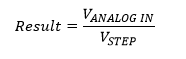
Step size is an analog voltage per unit of the ADC resolution.
For VREF+ = +5 V (VDD) and the VREF- = 0 V (VSS), we get the step size of
For example if the ADC result equal to 512, the voltage is,
Similarly, we get find the digital result equivalent to the analog input voltage,
In this example, I use a POT to adjust the analog input voltage varies from 0 to +5 V. To find the voltage we can use the equations listed above. But we can use another short form as,
In the C program, we must use the floating point to measure the analog voltage.
Schematic diagram. RB0 is AN12 analog input, measuring the input voltage
from 0 to +5 V. PORTC and PORTD display the measuring voltage with
one floating point.
The C source code:
#include<xc.h>
// PIC16F887 Configuration Bit Settings
// CONFIG1
#pragma config FOSC = XT
#pragma config WDTE = OFF
#pragma config PWRTE = OFF
#pragma config MCLRE = ON
#pragma config CP = OFF
#pragma config CPD = OFF
#pragma config BOREN = ON
#pragma config IESO = ON
#pragma config FCMEN = ON
#pragma config LVP = ON
// CONFIG2
#pragma config BOR4V = BOR40V
#pragma config WRT = OFF
/*_XTAL_FREQ use for __delay*/
#define _XTAL_FREQ 4000000

void driveDisplays(unsigned int analogRead){
 unsigned char ssd[16]={0x3F,0x06,0x5B,0x4F,0x66,0x6D,0x7D,
 0x07,0x7F,0x6F,0x77,0x7C,0x39,0x5E,0x79,0x71};
 float voltage;
 int _voltage;
 /*Voltage Calculation*/
 voltage=5*((float)analogRead/1024);
 _voltage=voltage*10;

 /*Decimal Place*/
 PORTD=0x00;
 PORTC=ssd[_voltage/10]|0x80;
 PORTD=0x01;
 __delay_ms(10);
 /*Floating point*/
 PORTD=0x00;
 PORTC=ssd[_voltage%10];
 PORTD=0x02;
 __delay_ms(10);
}
unsigned int readADC(void){
    GO=1;
    while(GO);
    __delay_ms(10);
    return (ADRESH<<8)+ADRESL;
}
void main(void){
    unsigned int adcResult;
    /*Analog and digital Port
     Configuration*/
    PORTB=0x00;
    PORTC=0x00;
    PORTD=0x00;
    TRISB=0x01;
    TRISC=0x00;
    TRISD=0x00;
    /*Result is right justify*/
    ADFM=1;
    /*By default is analog,
     but again set it to analog*/
    ANS12=1;
    /*Select FRC Clock of ADC module*/
    ADCON0bits.ADCS=0x03;
    /*Turn on ADC Module*/
    ADON=1;
    /*Select AN12 RB0*/
    ADCON0bits.CHS=0b1100;
    /*initiate a conversion*/
    GO=1;
    /*Wait until GO=0 "done"*/
    while(GO);
    while(1){
        adcResult=readADC();
        driveDisplays(adcResult);
        __delay_ms(20);
    }
}
Simulation screen shot. The measuring voltage displays 3.9 V DC.