Introduction
ATMega32 uses a successive approximation ADC type a device analog inputs. It's 10-bit wise and has up to 8 input channels. In addition, it can handle up to 16 differential voltage input combinations. |
| Eight analog input channel of ATMega32 |
Eight analog channels are multiplexed with PortA digital pins. By default PortA is digital I/O. AVCC is supply voltage for ADC module. AREF pin is a positive analog voltage reference. But the voltage reference could be programmed to internally connected to a 2.56 V reference voltage.
The ADC clock source is driven from the MCU clock with the division factor from 2 to 128. For the 10-bit ADC reading result, the clock frequency work 50 kHz to 200 kHz. But only an 8-bit result is needed the clock frequency could take higher than 200 kHz.
Basically, to use ADC we have to deal with some registers.
- ADMUX
Reference selection register REFS[1:0], used for selecting the reference voltage. By default it's AREF pin. For more reference voltage selections, check the device datasheet.
ADC left adjust result ADLR, used for adjusting the 10-bit ADC result between right and left. By default it's right justified ('0').
Analog channel and gain selection bits MUX[3:0], used for selecting between any single ended input, differential input and gain setting. By default, it's single ended ADC0 input channel.
- ADCSRA
ADC enable ADEN, turn on the ADC module when it's set to '1'.
ADC start conversion ADSC, start the ADC conversion when it's set to '1'. This bit is also used for testing the progress of the conversion. When it's read '0', the conversion is completed.
ADC auto trigger enable ADATE, make the ADC conversion automatically start by any options (see the datasheet).
ADC interrupt flag ADIF, is set to '1' when the ADC conversion is completed.
ADC interrupt enable ADIE, when set to '1' the interrupt for ADC is enabled.
ADC prescaler select bits ADPS[2:0], used for select the clock source for ADC. it's driven from MCU clock with the scale factor between 2 to 128. By default it has a division factor of 2.
- ADCL and ADCH
The data register is a 10-bit pair of two 8-bit registers ADCL and ADCH. It's readable and writable. By default ADLAR = '0', the result is right-justified.
Using the ADC
Basically, to program the ADC we must do the following steps:
- set the preferred pin to input
- in the ADMUX register, set the reference voltage, set up the result arrangement and select the analog input channel.
- in the ADCSRA register, turn on the ADC by setting ADEN to '1'. Selecting the ADC clock prescaler by setting any value to ADPS[1:0]
- start the conversion by setting the ADSC of the ADCSRA to '1'.
- wait for completion by checking the ADSC bit become low, or waiting for ADIF is activated.
- get the result from ADCL and ADCH.
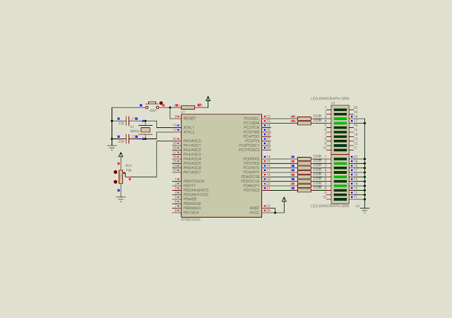
In this simple introduction of using the ADC, I use ADC0 an analog input channel with single end mode. The ADC clock is driven from the MCU clock with the division of 2. PortC displays the ADCH while PortD displays the ADCL result.
 |
| Schematic diagram. ATMega32 run at 4 MHz reading the analog input from ADC0. |
Source code:
#include <avr/io.h>
int main(void)
{
    //PortC as output
 DDRC=0xFF;
 //PortD as output
 DDRD=0xFF;
 //PA0 or ADC0 as an analog input
 DDRA=0;
 //Turn on the ADC module
 ADCSRA|=(1<<ADEN);
    while (1)
    {
  //Start the conversion
  ADCSRA|=(1<<ADSC);
  //Wait for the completion
  while((ADCSRA&(1<<ADSC))==1);
  //Read the result
  PORTD=ADCL;
  PORTC=ADCH;
    }
}
 |
| A screen shot simulation |
Click here to download its source file. Back to main tutorial page ATMega32 tutorials in C with Atmel Studio 7.


No comments:
Post a Comment