Learn To Write Code For 8051, Arduino, AVR, dsPIC, PIC, STM32 ARM Microcontroller, etc.
Coding Embedded Controller With C/C++.
Printed Circuit Board (PCB) Project For Electronics Hobbyists.
Using a prototype board for micro-controller firmware testing could save time and safer. Putting an on-board device programmer with prototype board could be more satisfy for electronic hobbyists.
I have some PIC18 and PIC16 series of micro-controllers left from previous projects. I don't know what to do with them anymore. So I put them on single board to PIC program testing next time I need them without checking their pin diagram, and wiring them on bread board.
PCB Front View
PCB Back View
I designed a PCB with a
PICKit2 device programmer (with AVR ISP header)
+5VDC and +3.3VDC low drop out power supply
RS-232 to TTL logic converter
I2C DS1307 RTC and 24LC08 EEPROM
4-bit LCD (HD4478)
3-digit 056'common cathode multiplexing display
One passive buzzer with transistor driver (using CCP1 PWM output pin of PIC16F876A)
8-LED that connects to PORTC of PIC16F876A
A 4x4 keypad matrix that connects to PORTB of PIC16F876A
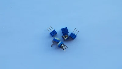
Three analog inputs (one LM35 and two potentiometers) that connect to RA0...RA1 of PIC16F876A.
A 28-pin IC socket for 28-pin PIC devices
A 20-pin IC socket for 20-pin PIC devices
A 18-pin IC socket for 18-pin PIC devices
A 14-pin IC socket for 14-pin PIC devices
And a 8-pin IC socket for 8-pin PIC devices
This board seem to be a large PCB with two copper layer near a size of an A4 paper that I'm not yet fabricate it. It need a PCB fabrication service.
Schematic
I use Protues VSM Release 8.16 SP3 to design draw its circuit diagram. Some components are not in its original libraries. So I find and download some devices symbol, footprints and 3D objects from snapeda website. I separate its schematic into A4 sheets.
Sheet #1
Sheet #2
Sheet #3
Sheet #4
Sheet #5
This board could fit,
28-pin PIC microcontrollers: PIC16F876A, PIC16F886, etc.
20-pin PIC microcontrollers: PIC16F1459(USB), PIC16F690, etc.
18-pin PIC microcontrollers: PIC16F1827, PIC16F84A, PIC16F818, etc.
14-pin PIC microcontrollers: PIC16F630, PIC16F676, etc.
8-pin PIC microcontrollers: PIC12F629, PIC12F675, PIC12F683, etc.
These are some mid-range PIC micro-controllers I have at my own workshop.
Printed Circuit Board (PCB)
This board size is 8.02x6.30 inches that could be a little bit expensive to order from any professional PCB fabrication service. But if we need to use it with classmate or friend the share cost is cheaper.
Top Copper non-mirror
Bottom Copper
Top Silk
I preview this PCB on an online Gerber viewer software.
I have been using PCBWay for many years now. PCBWay fabricate PCBs at low cost,
fast processing time for only 24 hours, and fast delivery time using
any carrier options. This double side 10cmx10cm can be fabricate at only
5USD for 5 to 10pcs by PCBWay. It's a standard PCB with silk screen and
solder mask.
DS3232 is an I2C protocol based RTC (real time clock) with a digital temperature inside. Its RAM store date/time, temperature and also a general purpose SRAM space.
A sample of program simulation
The device works at +3.3 V designed to fit any portable low power electronic applications. It's a 20-pin SMD device, requiring only a few external components. A very precise 32.768 kHz internal oscillator creates a timing for the device date/time. To keep the time working whenever it's power off, an external coin battery needed to connect to the Vbat pin of the IC.
DS3232 IC And Pins Diagram
Each pin has its function as lists below.
Pins description of DS3232 from device's datasheet
The I2C Interface
Inter-integrated circuit (I2C) is a two-wire serial communication developed by Phillip. It has been implementing by many manufacturers.
For DS3232 this communication protocol could clocks up to 400 kHz from the master device. The device writing address is the same to DS1307. The writing address for this device is 0xD0 while the reading address is 0xD1.
Master MCU writes to DS3232
Master MCU reads from DS3232
This device also support continuous pointer reading mode, but I don't list them here due to a novice programming.
Address Map
Address map is a RAM space contains date/time, control, and SRAM space. Date/time and control registers ranges from 0x00 to 0x13, while the remanding 0x14 to 0xFF are the general SRAM registers.
Just like DS1307 the starting address of 0x00 is the second register.
Date/time registers are read/write, and continuous increase up on the clock pulses, addresses from 0x00 to 0x06. The control registers, set the device square wave out, alarm setting, temperature reading enable etc. The alarm settings have many options, I don't list them here.
The remanding SRAM is general-purpose to the user for temporary data storage.
Control Register
This register locates at 0x0E in RAM. It configures many operation of the device.
Control Register
BIT 7 - Enable Oscillator: When device is powered on it's set to '0' to enable the oscillator. Setting this bit to '1', the device switch off from the oscillator.
BIT 6 - Battery-backed Square-wave Enable: If not necessary do not access to this bit.
BIT 5 - Convert Temperature: Setting this bit to '1' to enable temperature conversion. The temperature is 10-bit wide, and will be list next. The conversion takes at least 2 mS.
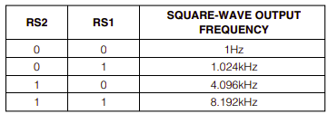
BIT 4:3 - Rate Select (RS2:1): They set the output frequency from INT/SQW pin.
Square-wave output frequency
BIT 2 - Interrupt Control: Setting this bit to 0 to enable the square wave output from INT/SQW pin.
BIT 1 - Alarm 2 Interrupt Enable: I don't use it here, please see the device's datasheet.
BIT 0 - Alarm 1 Interrupt Enable: I don't use it here, please see the device's datasheet.
This register also relate to control/status register.
Control/Status Register
This register locates at 0x0F. It contains some control and status bit.
BIT 7 - Oscillator Stop Flag: If it's '1' indicates that the oscillator is stop working.
BIT 6 - Battery-backed 32 kHz Output: If it's set to '1', it enable the 32 kHz output from the 32kHz pin when powered from the back up battery.
BIT 5:4 - Conversion Rate: These two bits determine the rate of temperature conversion (TCXO).
Conversion rate
BIT 3 - Enable 32 kHz Output: When this bit is set to '1' it enable the 32 kHz square wave output from the 32 kHz pin.
BIT 2 - BUSY: When this bit is read '1' indicates that the temperature conversion (TCXO) is not completed.
BIT 1 - Alarm 2 Flag: When it's set to '1' it indicates the time is matched in the alarm 2 register.
BIT 0 - Alarm 1 Flag: When it's set to '1' it indicates the time is matched in the alarm 1 register.
Temperature Registers
A digital thermometer is integrated inside the chip. Temperature data made of two bytes - the upper byte (0x11) and the lower byte(0x12).
At the upper byte the MSB bit 7 indicate the sign of temperature. When bit 7 is set to '1' it's at negative temperature environment. Then the upper temperature data must converter to 2'complement.
At the lower byte the two MSB bit indicate the fraction. It's 0.25 degree Celsius step.
SRAM
The SRAM is general purpose read/write RAM space for a user's temporary data storage. It ranges from 0x14 to 0xFF.
Interfacing And Programming.
With a software I2C library in CCS PICC, communicating with this device is pretty easy. Two SDA and SCL pins could be any pins within the I/O pin of the master MCU.
I selected RA0 and RA1 for SDA and SCL respectively.
Schematic Diagram
PIC16F716 clocks to 20 MHz, supplied at +5 V. DS3232 supplied at +3.3 V. Two resistor for data pins pull up to +3.3 V.
The LCD is 20x2 to fit all date/time and temperature data.
Today I just created a GitHub respiratory to store my working source codes.
CCS PICC source code is fed from my GitHub respiratory, lists below.
A real time clock (RTC) device creates current date and time. A precise oscillator synchronizes the timing of the RTC. A back up battery, typically a CR-2032 coin battery keeps the RTC alive when the system power supply is turned off.
Simulating Circuit For This Example
An RTC usually an external IC with SPI or I2C interface. An I2C interface has an advantage of using only two wires on a single bus, while an RTC with SPI interface requires more than two wires.
Maxim DS1307 is an RTC with I2C interface. It’s an 8-pin integrated circuit. It’s package has two options SO and PDIP. PDIP package is very useful in prototyping.
A piece of DS1307 I stock.
Pin diagram from device's datasheet
Each pin has their own name and functioning as lists below.
X1 – Crystal connection pin 1 : It’s connects to one pin of a 32.768kHz Quartz Crystal. It must by-pass a 12.5pF capacitor to the ground.
X2 – Crystal connection pin 2: It’s connects to one other pin of the 32.768kHz Quartz Crystal. It also require a by-pass capacitor.
VBAT – Backup supply input : It’s the positive pin of the backup battery, usually a 3V coin battery.
GND – Ground
SDA – Serial Data Input/Output : This data pin needs a pull-up resistor.
SCL – Serial Clock Input : This clock pin accepts clock pulse from the master I2C device. It also requires a pull-up resistor.
SQW/OUT- Square wave/output driver : This output pin generates an output square wave between 1 Hz to 32 kHz by software control.
VCC – Positive power supply – It work at typically +5 V DC.
The connection diagram to the microcontroller is shown below.
Typical circuit connection to MCU
Since the communication pins SCL(Serial Clock) and SDA(Serial Data) are open-drain, they require its own pull-up resistor, respectively. The resistance of the pull-up resistor is between 4.7 kOhm to 10 kOhm. For higher data rate we use a lower resistance.
Date and time data store in time-keeper registers. Each register is 8-bit wide with 64 rows.
RAM Registers From device's datasheet
From the address 0x00 to 0x06 are time registers. The 0x07 register is the control register. The remaining registers are RAM space.
The control register control the operation of SQW/OUT pin.
Control Register
Control register functions:
Bit 7 : OUT : This bit control the output level of SQW/OUT pin.
Bit 4 : SQWE (Square-wave Enable) : Setting this bit to ‘1’ allowing the output wave from SQW/OUT pin.
Bit 1 and Bit 0 are rate select bits
SQW rate selection bits
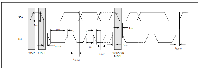
I do not list the details of I2C protocol here because there are a lot of resources on the web. The fundamental timing of the SDA and SCL pin list below.
I2C Timing Diagram
Writing to I2C device commonly send the address and send data. Reading from it means getting the data from the sent address.
Writing to DS1307
Reading from DS1307
The DS1307 write address is 0xD0 while the reading address is 0xD1.
Programming And Interfacing
Most microcontrollers shipped with I2C, allowing an easy interfacing to this device. But whenever any selected microcontroller has an absence of I2C, we must write a software-base I2C in any assembler or compiler.
CCS PICC compiler is a embedded C compiler targeting 8-bit and 16-bit PIC devices. It has a ready-to-use C function for I2C. Any device device with I2C, we can use a fast and robust hardware I2C library. However, for any device without I2C we must use a software I2C library with a select-able pins.
In this example, I use PIC16F716 in my closet. However, this PICMicro doesn’t have I2C module in its peripherals. I use software I2C library in the compiler. It’s fast and reliable.
PIC16F716-I/P 18-Pin DIP I use for my prototyping.
Data and time are read from ds1307 and display them on the 20×2 character LCD.
In the previous example, I show a simple method to rotate the angle of a servo motor using delay() function in CCS PICC.
Controlling a servo motor with PIC16F84A
In this example I use three potentiometers to adjust the three corresponding servo motor simultaneously.
A simple pot can generate variable analog voltage output, fed to the MCU analog input.
The overall process is to convert the 8-bit analog value reading from pot to PIC16F716. Then converting the 8-bit analog data to time value in microseconds.
The 8-bit data have 256 value. This 256 value map the 1000 microsecond high time.
The PIC16F716 CPU clocks at 20 Mhz, giving a precise timing for delay() function.
Three pots connect to RA0, RA1 and RA3.
Three servo output connect to RB0, RB1 and RB2.