Learn To Write Code For 8051, Arduino, AVR, dsPIC, PIC, STM32 ARM Microcontroller, etc.
Coding Embedded Controller With C/C++.
Printed Circuit Board (PCB) Project For Electronics Hobbyists.
In the previous post, I showed a 8-bit parallel port LCD interfacing with ATMega32 digital ports. However, as it's stated in the datasheet of HD44780, this controller could interface using only its four upper data bits (D4 to D7).
An example of using the LCD in 4-bit data lines.
In 4-bit data transfer mode, however the controller requires its full 8-bit instruction or LCD data. To send the 8-bit instruction or data, the connected MCU needs to send it twice.
The MCU sends the high nibble first
Finally the lower nibble shift left for four times and send it to the LCD D7:4 pins.
Timing diagram for 4-bit interfacing mode
By following, the JHD162A the step-by-step 4-bit LCD interfacing configuration shown below.
Both data and instruction bytes send the controller is the same to one's in the 8-bit mode. But they are separated to send twice as described above.
LCD Interfacing And Programming In 4-bit Mode
Using Two Distinct Ports
At this beginning example, I use two distinct port for LCD control pins and LCD data/instruction pins, respectively.
Schematic diagram for 4-bit LCD interfacing
The program display the time in days and HH:MM:SS since the MCU powered up. I fetch the source code from my GitHub gist respiratory below.
The simulation shows 1 minute and 38 seconds since the MCU powered up.
We can use a single port for LCD interfacing in some situations. The overall process is the same. But we must select any control pins in the same port.
Using A Single Port - Here I use a 20x4 LCD.
Source code fetched from gist.
Schematic Diagram For A Single Port Interfacing
Click here to download example archive. This character LCD can be driven by a serial to parallel shift registers. We can use these two chips - the SN74HC595 and the SN74HC164.
HD44780 is character LCD controller developed by Hitachi. It usually equipped with a Fax machine, a printer and photocopier machine.
This controller embedded in any LCD module with different number of lines and characters, a 8x1, a 16x1, a 16x2, or a 20x4 LCD module, etc. Currently, there are many equivalent controller to this old one's, for example a ST7066U and ST7065C controller.
A JHD162A 16x2 Character LCD Module
A 1602ZFA 16x2 LCD Module. This module uses both ST7066U and ST7065C controller, but it's compatible to HD44780 controller.
Interfacing With HD44780
This controller typically work at 5 V DC. Its communication to the MCU is in parallel mode - 8-bit or 4-bit data lines. Here I select JHD162A LCD module to work with.
JHD162A pins function
The data bus is 8-bit wide, with three control lines. The R/W uses for read and write. Usually, the programmer only need to write to the module, thus this pin must wires to the ground.
Register select (RS) pin is the module input, commanding the the controller to accept between instruction (command) and data. Command is any LCD instruction - clearing the display or returning home.
Enable (E) pin is the module input, the 8-bit data is fetch into the controller at the HIGH logic level of this pin.
Writing A Command To HD44780
Writing A Data To HD44780
The interfacing I talk here is 8-bit mode only. For the 4-bit interfacing, it will be discuss in the later post.
Internal RAM and ROM
Characters to display are any ASCII or Japanese characters. They are mask-programmed and creates by the character generator ROM (CGROM). The character could be in 5x8 or 5x10 dot.
The display data RAM (DDRAM) output the characters to LCD module display. DDRAM size varies depend on the number of lines and characters of the module.
Any custom characters outside the pre-build character of the module could be created using the character generator RAM. The process of creating the custom character is not discuss here.
LCD Configuring And Displaying A Character
Displaying a character need an initial LCD configuration. Configuration is made by writing some LCD command to the module with some preferred commands. After the configuration is done, the character is displayed by sending the data (ASCII character) to the module.
There are many commands for this controller.
All instructions set from JHD162A datasheet.
Each writing the controller requires a time of at least 40 micro seconds to a few milli seconds a listed in the table above.
There are many types of this module, hence its DDRAM are different in size.
A 16x2 LCD Type
- Line 1 starts from the address 0x80 to 0x8F.
- Line 2 starts from the address 0xC0 to 0xCF.
A 20x1 LCD Type
- Line 1 starts from the address 0x80 to 0x93.
A 20x2 LCD Type
- Line 1 starts from the address 0x80 to 0x93.
- Line 2 starts from the address 0xC0 to 0xD3.
A 20x4 LCD Type
- Line 1 starts from the address 0x80 to 0x93.
- Line 2 starts from the address 0xC0 to 0xD3.
- Line 3 starts from the address 0x94 to 0xA7.
- Line 4 starts from the address 0xD4 to 0xE7.
A 40x2 LCD Type
- Line 1 starts from the address 0x80 to 0xA7.
- Line 2 starts from the address 0xC0 to 0xE7.
This information I got from an AVR microcontroller book.
Interfacing And Programming With ATMega32
Example 1
I follow the controller operation example from its datasheet. The scrapped operational steps in the picture below.
It use the 8-bit data mode for a 8x1 LCD type. However, I use JHD162A with instead due to its availability.
Schematic Diagram
I clock the ATMega32 to 16 MHz due to an on-board oscillator. The 8-bit data connects to PORTD. The control pins connect to PORTC.
The programming example below use the 8-bit interfacing mode to display the text "A.K.I". Each character display has a delay of 2 seconds. Source codes of this example is fetch from my GitHub gist respiratory.
A simulation screen shot shown below.
A simulation screen shot of this example, The display shows the text "A.K.I".
I stored a zip file of this example in my GitHub respiratory here.
Example 2
In this example, I use this 16x2 LCD to display text at on all the two lines of the display. We set the cursor to auto increment by 1, then it moves to next DDRAM address. Additionally, a C pointer is a dynamic RAM addressing. Increasing the pointer, to space up the data size in the unit of 8-bit. With this advantage, we can write a continuous text string to the display without writing each character one by one as we have done in the previous example.
I add a new function. It relies on writeCharacter() function.
void writeString(char *text){
while(*text) writeChararacter(*text++);
}
The display show time in seconds since the MCU powered up. It counts the time in seconds - from 0 to 255 because I use only an 8-bit "char" data type.
I fetch the source codes from my GitHub gist directory.
The simulation result is shown below.
The time counts reaches 200 seconds since the MCU powered up.
Example 3
I have read the AVR microcontroller book. I got some techniques from that. We can set the position of the cursor easily by writing an additional function. This function set the DDRAM address on the display.
In the source code I name this function to setXy().
/*This function ease of setting the cursor position*/
void setXy(int x,int y){
char numberOfLines[2]={0x80,0xC0};
/* The position starts from (x,y)=(0,0) */
writeCommand(numberOfLines[x]+y);
}
The source codes is updated as follow.
The program remains the same in schematic diagram, except an additional setXy function and some displaying texts.
There is another simple serial to parallel shift register chip that need only two pins - serial data and serial clock. It's the SN74HC164. This chip also able to drive this LCD in 4-bit or 8-bit mode. However it requires a few microcontroller control pins beside the two serial pins. For 4-bit mode we will need to add E(Enable) pin that drive from any microcontroller pin.
DS3232 is an I2C protocol based RTC (real time clock) with a digital temperature inside. Its RAM store date/time, temperature and also a general purpose SRAM space.
A sample of program simulation
The device works at +3.3 V designed to fit any portable low power electronic applications. It's a 20-pin SMD device, requiring only a few external components. A very precise 32.768 kHz internal oscillator creates a timing for the device date/time. To keep the time working whenever it's power off, an external coin battery needed to connect to the Vbat pin of the IC.
DS3232 IC And Pins Diagram
Each pin has its function as lists below.
Pins description of DS3232 from device's datasheet
The I2C Interface
Inter-integrated circuit (I2C) is a two-wire serial communication developed by Phillip. It has been implementing by many manufacturers.
For DS3232 this communication protocol could clocks up to 400 kHz from the master device. The device writing address is the same to DS1307. The writing address for this device is 0xD0 while the reading address is 0xD1.
Master MCU writes to DS3232
Master MCU reads from DS3232
This device also support continuous pointer reading mode, but I don't list them here due to a novice programming.
Address Map
Address map is a RAM space contains date/time, control, and SRAM space. Date/time and control registers ranges from 0x00 to 0x13, while the remanding 0x14 to 0xFF are the general SRAM registers.
Just like DS1307 the starting address of 0x00 is the second register.
Date/time registers are read/write, and continuous increase up on the clock pulses, addresses from 0x00 to 0x06. The control registers, set the device square wave out, alarm setting, temperature reading enable etc. The alarm settings have many options, I don't list them here.
The remanding SRAM is general-purpose to the user for temporary data storage.
Control Register
This register locates at 0x0E in RAM. It configures many operation of the device.
Control Register
BIT 7 - Enable Oscillator: When device is powered on it's set to '0' to enable the oscillator. Setting this bit to '1', the device switch off from the oscillator.
BIT 6 - Battery-backed Square-wave Enable: If not necessary do not access to this bit.
BIT 5 - Convert Temperature: Setting this bit to '1' to enable temperature conversion. The temperature is 10-bit wide, and will be list next. The conversion takes at least 2 mS.
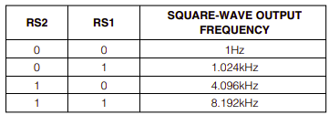
BIT 4:3 - Rate Select (RS2:1): They set the output frequency from INT/SQW pin.
Square-wave output frequency
BIT 2 - Interrupt Control: Setting this bit to 0 to enable the square wave output from INT/SQW pin.
BIT 1 - Alarm 2 Interrupt Enable: I don't use it here, please see the device's datasheet.
BIT 0 - Alarm 1 Interrupt Enable: I don't use it here, please see the device's datasheet.
This register also relate to control/status register.
Control/Status Register
This register locates at 0x0F. It contains some control and status bit.
BIT 7 - Oscillator Stop Flag: If it's '1' indicates that the oscillator is stop working.
BIT 6 - Battery-backed 32 kHz Output: If it's set to '1', it enable the 32 kHz output from the 32kHz pin when powered from the back up battery.
BIT 5:4 - Conversion Rate: These two bits determine the rate of temperature conversion (TCXO).
Conversion rate
BIT 3 - Enable 32 kHz Output: When this bit is set to '1' it enable the 32 kHz square wave output from the 32 kHz pin.
BIT 2 - BUSY: When this bit is read '1' indicates that the temperature conversion (TCXO) is not completed.
BIT 1 - Alarm 2 Flag: When it's set to '1' it indicates the time is matched in the alarm 2 register.
BIT 0 - Alarm 1 Flag: When it's set to '1' it indicates the time is matched in the alarm 1 register.
Temperature Registers
A digital thermometer is integrated inside the chip. Temperature data made of two bytes - the upper byte (0x11) and the lower byte(0x12).
At the upper byte the MSB bit 7 indicate the sign of temperature. When bit 7 is set to '1' it's at negative temperature environment. Then the upper temperature data must converter to 2'complement.
At the lower byte the two MSB bit indicate the fraction. It's 0.25 degree Celsius step.
SRAM
The SRAM is general purpose read/write RAM space for a user's temporary data storage. It ranges from 0x14 to 0xFF.
Interfacing And Programming.
With a software I2C library in CCS PICC, communicating with this device is pretty easy. Two SDA and SCL pins could be any pins within the I/O pin of the master MCU.
I selected RA0 and RA1 for SDA and SCL respectively.
Schematic Diagram
PIC16F716 clocks to 20 MHz, supplied at +5 V. DS3232 supplied at +3.3 V. Two resistor for data pins pull up to +3.3 V.
The LCD is 20x2 to fit all date/time and temperature data.
Today I just created a GitHub respiratory to store my working source codes.
CCS PICC source code is fed from my GitHub respiratory, lists below.
A real time clock (RTC) device creates current date and time. A precise oscillator synchronizes the timing of the RTC. A back up battery, typically a CR-2032 coin battery keeps the RTC alive when the system power supply is turned off.
Simulating Circuit For This Example
An RTC usually an external IC with SPI or I2C interface. An I2C interface has an advantage of using only two wires on a single bus, while an RTC with SPI interface requires more than two wires.
Maxim DS1307 is an RTC with I2C interface. It’s an 8-pin integrated circuit. It’s package has two options SO and PDIP. PDIP package is very useful in prototyping.
A piece of DS1307 I stock.
Pin diagram from device's datasheet
Each pin has their own name and functioning as lists below.
X1 – Crystal connection pin 1 : It’s connects to one pin of a 32.768kHz Quartz Crystal. It must by-pass a 12.5pF capacitor to the ground.
X2 – Crystal connection pin 2: It’s connects to one other pin of the 32.768kHz Quartz Crystal. It also require a by-pass capacitor.
VBAT – Backup supply input : It’s the positive pin of the backup battery, usually a 3V coin battery.
GND – Ground
SDA – Serial Data Input/Output : This data pin needs a pull-up resistor.
SCL – Serial Clock Input : This clock pin accepts clock pulse from the master I2C device. It also requires a pull-up resistor.
SQW/OUT- Square wave/output driver : This output pin generates an output square wave between 1 Hz to 32 kHz by software control.
VCC – Positive power supply – It work at typically +5 V DC.
The connection diagram to the microcontroller is shown below.
Typical circuit connection to MCU
Since the communication pins SCL(Serial Clock) and SDA(Serial Data) are open-drain, they require its own pull-up resistor, respectively. The resistance of the pull-up resistor is between 4.7 kOhm to 10 kOhm. For higher data rate we use a lower resistance.
Date and time data store in time-keeper registers. Each register is 8-bit wide with 64 rows.
RAM Registers From device's datasheet
From the address 0x00 to 0x06 are time registers. The 0x07 register is the control register. The remaining registers are RAM space.
The control register control the operation of SQW/OUT pin.
Control Register
Control register functions:
Bit 7 : OUT : This bit control the output level of SQW/OUT pin.
Bit 4 : SQWE (Square-wave Enable) : Setting this bit to ‘1’ allowing the output wave from SQW/OUT pin.
Bit 1 and Bit 0 are rate select bits
SQW rate selection bits
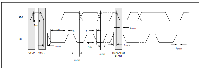
I do not list the details of I2C protocol here because there are a lot of resources on the web. The fundamental timing of the SDA and SCL pin list below.
I2C Timing Diagram
Writing to I2C device commonly send the address and send data. Reading from it means getting the data from the sent address.
Writing to DS1307
Reading from DS1307
The DS1307 write address is 0xD0 while the reading address is 0xD1.
Programming And Interfacing
Most microcontrollers shipped with I2C, allowing an easy interfacing to this device. But whenever any selected microcontroller has an absence of I2C, we must write a software-base I2C in any assembler or compiler.
CCS PICC compiler is a embedded C compiler targeting 8-bit and 16-bit PIC devices. It has a ready-to-use C function for I2C. Any device device with I2C, we can use a fast and robust hardware I2C library. However, for any device without I2C we must use a software I2C library with a select-able pins.
In this example, I use PIC16F716 in my closet. However, this PICMicro doesn’t have I2C module in its peripherals. I use software I2C library in the compiler. It’s fast and reliable.
PIC16F716-I/P 18-Pin DIP I use for my prototyping.
Data and time are read from ds1307 and display them on the 20×2 character LCD.
NXP PCF8574 is a remote digital inputs outputs expander. The interfacing method is implemented using the two-wire Inter Integrated Circuit (I2C) with the frequency up to 100 kHz. It has an 8-bit digital input output port. It's input output port is quasi-bidirectional. It does not require direction control.
A sample of program PIC12F629 connects to PCF8574 via software I2C Interface
Samples of PCF8574AP I bought from on line store
PCF8574AP Pin Diagram
Each pin of this 16-pin DIP device lists below.
Pin description of PCF8574 (from datasheet)
Supply voltage for this device ranges from 2.5 V to 6 V, typically 5 V for hobbyist prototyping. It's commonly found in input/output driving, keypad, and character LCD interface converter.
Programming For PCF8574
To interface to I2C devices on bus, we must know about it's device read/write address follows by an I2C start condition. It's read/write address varied with three bits A2, A1 and A0. These three pins must pull high or low externally, to make a specific slave address. The address lists below.
PCF8574 slave address
With these three bits, we could make three different slave address.
PCF8574 address map
Writing to the port of PCF8574 make its digital port as output. After a start condition, we must send the device slave address as listed above, follows by an 8-bit output value.
Write mode (output)
To read from this device, we put its read address, follows by data reading. For example, when we connect A2, A1 and A0 to VSS the device write address is 0x40 with the read address 0x41.
The INT (interrupt) pin is an output from PCF8574. It's open drain. This pin create a low signal when there's any logic state changed at input to the port of PCF8574.
Connecting the INT to Microcontroller
CCS PICC Coding
CCS PICC is a C compiler for 8-bit and 16-bit PICMicro. It's fast and easy to use with a lot of library. There are both hardware and software library. In the case of I2C, any device with I2C (for example PIC16F818) we can use hardware library or software library. Hardware I2C library is fast and reliable. Software I2C library work slower because it use program routine. Sometimes, it cause data corrupt. But with software I2C library, we can select any two-pin within the device.
PIC12F629 is an 8-pin 8-bit PICMicro in the Mid-Range family. It doesn't have I2C module shipped. However, we can use software I2C library instead.
Pin Diagram
In this example, I read data from the lower nibble of PCF8574 input and output to its higher nibble to the port.
Schematic Diagram
Source Code.
#include<12F629.h>
/*Use internal RC oscillator*/
#fuses INTRC_IO
#use delay(clock=4M)
/*implementing the software-base I2C*/
#use i2c(scl=pin_a0,sda=pin_a1,FORCE_SW)

void main(void){
   char rcvData=0;

   while(1){
      /*Turn on lower nibble high
      for digital input*/
      i2c_start();
      i2c_write(0x40);
      i2c_write(rcvData|0x0F);
      i2c_stop();

      /*Read the input state of
      lower nibble*/
      i2c_start();
      i2c_write(0x41);
      rcvData=i2c_read();
      i2c_stop();

      /*Shift the inputs right
      to the output*/
      rcvData<<=4;

      /*Write Data to output*/
      i2c_start();
      i2c_write(0x40);
      i2c_write(0x0F);
      i2c_stop();

      /*Turn on lower nibble high
      for digital input*/
      i2c_start();
      i2c_write(0x40);
      i2c_write(rcvData|0x0F);
      i2c_stop();

      /*wait for 100 mS*/
      delay_ms(100);
   }
}
Click here to download the complete example. This example uses the ATMega32 to interfaces with the PCF8574A using its TWI module.