Sunday, April 25, 2021

PIC18f2550 RS-232 Programming example in CCS PICC

In previous post, we showed a DIY prototyping board for PIC18F2550. That board has a block of RS-232 to TTL converter but it was not tested. We will test that block here separately. 

CCS PICC has a built-in library of RS-232. It doesn't need to configure all related registers in SFR to make this module work. Its primary task is to add the #use rs232() directive in source code. This directive needs the #use delay(clock=x) directive to be declared first. For example,

#use delay (clock=4M)
#use RS232(uart1,baud=9600)

C directive showed above inform the compiler to use 4MHz clock frequency. Default UART is uart1 for most of PIC micro-controller that come with USART module inside. The baud rate is set to 9600.

UART communication for 8-bit are RC6 for transmission (Tx), and RC7 for reception (Rx). UART data I/O functions are just like the ANSI C library function. For example printf() is use for outputting ASCII data from micro-controller from its Tx pin. Other ANSI C functions are usable in CCS PICC such as getc(), putc(), kbhit(), etc.

This example will show how to use these RS-232 functions with PIC18F2550 micro-controller.

#include <18f2550.h>
//use external 20MHz crystal oscillator 
#fuses HS,NOWDT,PLL1,CPUDIV1
#use delay(clock=20M)
#use rs232(uart1,baud=9600)

void main(void){
   char temp1=0;
   //Clear PortC
   output_C(0x00);
   //PortC as output
   set_tris_C(0x00);
   printf("PIC18F2550 USB Board\n\r");
   printf("Please enter number between 0 and 3\n\r");
   printf("to toggle RC1 and RC2.\n\r");
   while(1){    
   //Test buffer
      if(kbhit()){
            temp1=getc();
            putc(temp1);
      }
      switch(temp1){
         case '0':
            output_low(pin_c1);
            temp1=0;
            printf("\tRC1 is OFF.\n\r");
            break;
         case '1':
            output_high(pin_c1);
            temp1=0;
            printf("\tRC1 is ON.\n\r");
            break;
         case '2':
            output_low(pin_c2);
            temp1=0;
            printf("\tRC2 is OFF.\n\r");
            break;
         case '3':
            output_high(pin_c2);
            temp1=0;
            printf("\tRC2 is ON.\n\r");
            break;
         case 0:
            break;
         default:
            printf("\n\rPlease enter number between 0 and 3\n\r");
            printf("to toggle RC1 and RC2.\n\r");
            temp1=0;
            break;
      }
   }
}

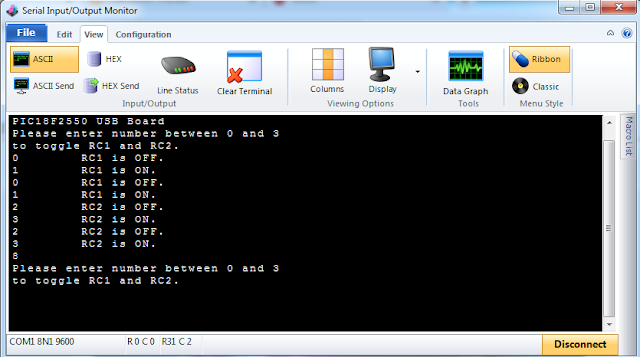
I tested this example on my prototyping board.

PIC18f2550 RS-232 Programming example in CCS PICC
Program testing on prototyping board

PIC18f2550 RS-232 Programming example in CCS PICC
Host PC and PIC18F2550 side sending/receive data

I run this testing using a desktop PC with COM port on Windows 7 64-bit. The serial terminal showed above is a part of CCS PICC compiler IDE.

Monday, April 19, 2021

DIY PIC18F2550 USB Board

Introduction

PIC18F2550 provides Universal Serial Bus (USB) communication interface, up to 12Mbit/s Full Speed USB 2.0. It can clock up to 48MHz with 12MIPS executing speed using its Phase Lock Loop (PLL) module. This 28-pin USB slave device operates between 2 to 5.5V. Using 5V DC supply voltage allows this chip to operate at its optimal performance.

Unlike Arduino or NXP micro-controllers, this device doesn't come with boot-loader. An external In Circuit System Programmer (ICSP) is needed to burn its firmware into device's internal flash memory. An earlier version of PICKit USB programmer/debugger is a popular low cost device programmer. PICKit2 is very popular due to its price. However it's easy to build for electronics hobbyists. I tried to make this programmer by myself as I was a university student.

Using micro-controller development board would save the prototyping time. However we can assemble a testing board for this micro-controller individually. Assembling device programmer and target testing micro-controller on a single board could be a good way, but it will cost more money and design space.


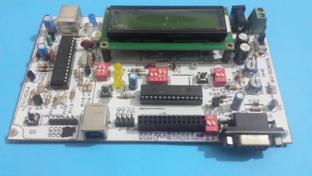
DIY PIC18F2550 USB Board
A ready to use prototyping board for PIC18F2550

This testing board is already assembled and tested. However it has some fault during the design. I corrected all the on board mistakes and schematic/PCB design. 

PCB design and processing

I made schematic and PCB design by myself. Printed circuit was fabricated using a DIY low cost toner transfer method with an in house laser printer. It takes a few days to complete the design, DIY PCB processing, and assembling of all on-board components.

PCB Processing

DIY PIC18F2550 USB Board
Copper clad board with transferred circuit pattern
Laser photo paper, glossy paper produces a good result of circuit pattern transferring. As it's shown on this picture above, the black circuit pattern is laser printer toner that will protect the circuit pattern during acid etching. 

DIY PIC18F2550 USB Board
Circuit board after PCB etching

DIY PIC18F2550 USB Board
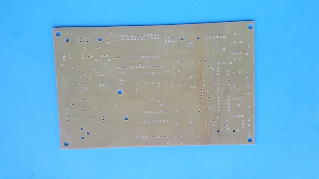
PCB panel after drilling

It takes around 5 minutes to finish PCB etching. Ferric Chloride is a low cost etching chemical for DIY PCB processing.

DIY PIC18F2550 USB Board
Back panel of PCB
Copper clad board is fiber glass FR-4 type. Its back panel is light green in color. I sprayed it with white acrylic paint. Component legends that stick on its panel is laser printer black toner.

DIY PIC18F2550 USB Board
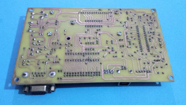
Prototyping board after assembling

PCB soldering seem to be untidy due to unwell copper track protection during etching. However it doesn't matter for hobbyists.

DIY PIC18F2550 USB Board
Components side after PCB assembling

Schematic and PCB Design

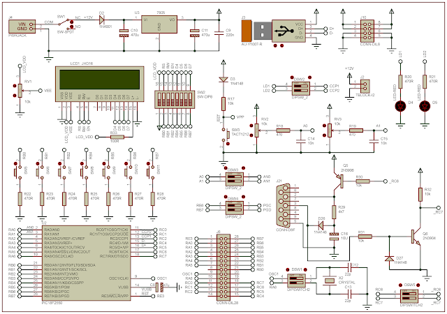
Schematic design makes up to two design sheet in A4 paper side. One's for PICKit2 device programmer and one's for PIC18F2550 testing board. Schematic for PICKit2 will not be shown here due to its untidiness, but it works.

DIY PIC18F2550 USB Board
Schematic for testing board
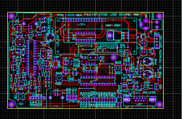
Finished circuit design is a single sided PCB. It has some wire jumpers on its back panel.
 
DIY PIC18F2550 USB Board
PCB Design View

I use top copper layer in red color as copper side due to my previous design of PICKit 2 device programmer.

DIY PIC18F2550 USB Board
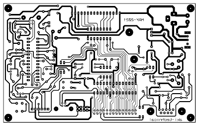
PCB copper side - non-mirror

It will need some wire jumpers on components side as shown on the picture below.

DIY PIC18F2550 USB Board
Components side and wire jumpers - mirror

There are some essential blocks on this board:

  1. PICKit2 device programmer/debugger with external programming header, and DIP switch connects to on-board target PIC device
  2. Regulated +5V DC supply from external DC voltage input
  3. Character LCD connects to PortB in 4-bit mode via DIP switch
  4. Two on-board testing LED(s) connect to RC1 and RC2, enable/disable by DIP switch
  5. One active low tactile switch connects to RB0 of PortB
  6. USB connector for USB connection to host computer
  7. Two trimmer Pots connect to AN0 and AN1, enable/disable by a DIP switch
  8. RS-232 connector with Tx/Rx pair for UART programming
  9. PIC18F2550 microcontroller with reset circuit, and a crystal oscillator with a frequency of 20MHz.

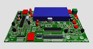
DIY PIC18F2550 USB Board
3D view of PCB design

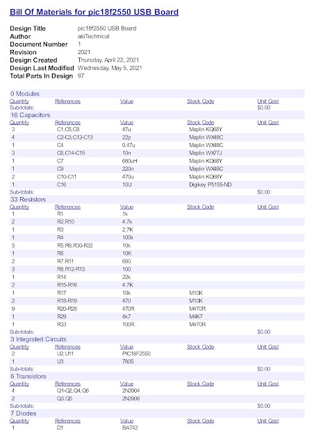
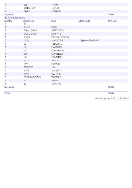
This prototype requires 97 necessary components as it's listed in Bill Of Materials (BOM).

Bill Of Materials (BOM)

Bill Of Materials (BOM)
Design file could be download here.

Board and Program Testing

PICKit2 Device Programmer Testing

On this prototyping board, PICKit2 works at +5V DC supplied from USB bus voltage. It works well at fixed +5V voltage.

DIY PIC18F2550 USB Board
This is a screen shot of device programming on Windows 7 x64 host PC while this prototyping board connects onUSB.

This device programmer is able to power overall system on prototyping board.

Character LCD Test

Character LCD connects to PortB of PIC18F2550 in 4-bit interfacing mode. I test this block using CCS PICC compiler due to its ease of programming.

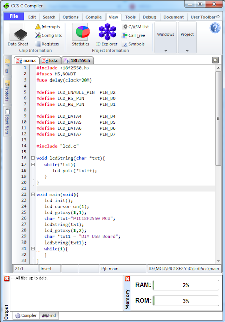
DIY PIC18F2550 USB Board
LCD Testing using CCS PICC Program

The program below is its source code in text format.


#include <18f2550.h>
#fuses HS,NOWDT
#use delay(clock=20M)
   
#define LCD_ENABLE_PIN  PIN_B2
#define LCD_RS_PIN      PIN_B0                                   
#define LCD_RW_PIN      PIN_B1   

#define LCD_DATA4       PIN_B4                                    
#define LCD_DATA5       PIN_B5                                    
#define LCD_DATA6       PIN_B6                                    
#define LCD_DATA7       PIN_B7 

#include "lcd.c"

void lcdString(char *txt){
   while(*txt){
      lcd_putc(*txt++);
   }
}

void main(void){
   lcd_init();
   lcd_cursor_on(1);
   lcd_gotoxy(1,1);
   char *txt="PIC18F2550 MCU";
   lcdString(txt);
   lcd_gotoxy(1,2);
   char *txt1 = "DIY USB Board";
   lcdString(txt1);
   while(1){
   }
}

During device uploading please open SW2 DIP switch, or remove LCD module. DSW4 DIP switch must be closed to enable PGC and PGD of PICKit2 programming header.

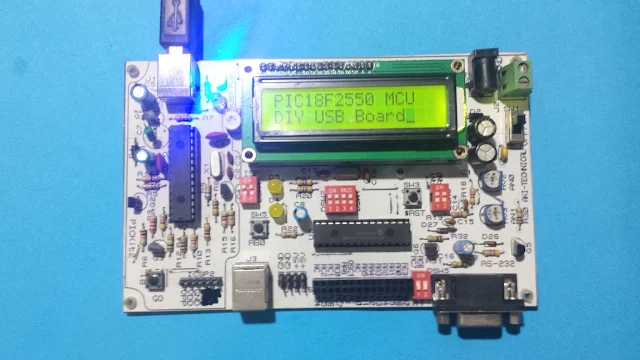
DIY PIC18F2550 USB Board
Character LCD testing 

After PICKit2 device uploading please disconnect DSW4, and enable LCD header using SW2.

On-board LED Testing

Two LED(s) connect to RC1 and RC2 of PortC. They are enabled/disabled by DSW2 DIP switch. 


/*
 * LED(s) testing on PIC18F2550 USB Board
 * Testing program is written using MPLABX
 * XC8 C compiler for 8-bit PIC.
 */
#include <xc.h>
#include "configPic18f2550.h"

/*Clock frequency parameter for delay function
 *Microcontroller operates at 20MHz from external
 *crystal oscillator
 */
#define _XTAL_FREQ  20e6

/*LED(s) labels*/
#define LED1    RC1
#define LED1Dir TRISC1
#define LED2    RC2
#define LED2Dir TRISC2

void myDelay(unsigned int _ms){
    for(unsigned int i=0;i<_ms;i++)
    __delay_ms(1);
}
int main(void){
    /*Clear PortC*/
    PORTC=0x00;
    /*LED1 output direction*/
    LED1Dir=0;
    /*LED2 output direction*/
    LED2Dir=0;
    while(1){
        LED1=0;
        LED2=1;
        myDelay(1000);
        LED1=1;
        LED2=0;
        myDelay(1000);
    }
}

XC8 configuration file for PIC18F2550 contain many lines of embedded C directive. I separate this configuration words in one C header file with project folder.

/* 
 * File:   configPic18f2550.h
 * Author: admin
 *
 * Created on May 5, 2021, 10:39 AM
 */

#ifndef CONFIGPIC18F2550_H
#define CONFIGPIC18F2550_H


#endif /* CONFIGPIC18F2550_H */


// PIC18F2550 Configuration Bit Settings

// CONFIG1L
#pragma config PLLDIV = 1       // PLL Prescaler Selection bits (No prescale (4 MHz oscillator input drives PLL directly))
#pragma config CPUDIV = OSC1_PLL2// System Clock Postscaler Selection bits ([Primary Oscillator Src: /1][96 MHz PLL Src: /2])
#pragma config USBDIV = 1       // USB Clock Selection bit (used in Full-Speed USB mode only; UCFG:FSEN = 1) (USB clock source comes directly from the primary oscillator block with no postscale)

// CONFIG1H
#pragma config FOSC = HS        // Oscillator Selection bits (HS oscillator (HS))
#pragma config FCMEN = OFF      // Fail-Safe Clock Monitor Enable bit (Fail-Safe Clock Monitor disabled)
#pragma config IESO = OFF       // Internal/External Oscillator Switchover bit (Oscillator Switchover mode disabled)

// CONFIG2L
#pragma config PWRT = OFF       // Power-up Timer Enable bit (PWRT disabled)
#pragma config BOR = ON         // Brown-out Reset Enable bits (Brown-out Reset enabled in hardware only (SBOREN is disabled))
#pragma config BORV = 3         // Brown-out Reset Voltage bits (Minimum setting)
#pragma config VREGEN = OFF     // USB Voltage Regulator Enable bit (USB voltage regulator disabled)

// CONFIG2H
#pragma config WDT = OFF        // Watchdog Timer Enable bit (WDT disabled (control is placed on the SWDTEN bit))
#pragma config WDTPS = 32768    // Watchdog Timer Postscale Select bits (1:32768)

// CONFIG3H
#pragma config CCP2MX = ON      // CCP2 MUX bit (CCP2 input/output is multiplexed with RC1)
#pragma config PBADEN = ON      // PORTB A/D Enable bit (PORTB<4:0> pins are configured as analog input channels on Reset)
#pragma config LPT1OSC = OFF    // Low-Power Timer 1 Oscillator Enable bit (Timer1 configured for higher power operation)
#pragma config MCLRE = ON       // MCLR Pin Enable bit (MCLR pin enabled; RE3 input pin disabled)

// CONFIG4L
#pragma config STVREN = ON      // Stack Full/Underflow Reset Enable bit (Stack full/underflow will cause Reset)
#pragma config LVP = OFF        // Single-Supply ICSP Enable bit (Single-Supply ICSP disabled)
#pragma config XINST = OFF      // Extended Instruction Set Enable bit (Instruction set extension and Indexed Addressing mode disabled (Legacy mode))

// CONFIG5L
#pragma config CP0 = OFF        // Code Protection bit (Block 0 (000800-001FFFh) is not code-protected)
#pragma config CP1 = OFF        // Code Protection bit (Block 1 (002000-003FFFh) is not code-protected)
#pragma config CP2 = OFF        // Code Protection bit (Block 2 (004000-005FFFh) is not code-protected)
#pragma config CP3 = OFF        // Code Protection bit (Block 3 (006000-007FFFh) is not code-protected)

// CONFIG5H
#pragma config CPB = OFF        // Boot Block Code Protection bit (Boot block (000000-0007FFh) is not code-protected)
#pragma config CPD = OFF        // Data EEPROM Code Protection bit (Data EEPROM is not code-protected)

// CONFIG6L
#pragma config WRT0 = OFF       // Write Protection bit (Block 0 (000800-001FFFh) is not write-protected)
#pragma config WRT1 = OFF       // Write Protection bit (Block 1 (002000-003FFFh) is not write-protected)
#pragma config WRT2 = OFF       // Write Protection bit (Block 2 (004000-005FFFh) is not write-protected)
#pragma config WRT3 = OFF       // Write Protection bit (Block 3 (006000-007FFFh) is not write-protected)

// CONFIG6H
#pragma config WRTC = OFF       // Configuration Register Write Protection bit (Configuration registers (300000-3000FFh) are not write-protected)
#pragma config WRTB = OFF       // Boot Block Write Protection bit (Boot block (000000-0007FFh) is not write-protected)
#pragma config WRTD = OFF       // Data EEPROM Write Protection bit (Data EEPROM is not write-protected)

// CONFIG7L
#pragma config EBTR0 = OFF      // Table Read Protection bit (Block 0 (000800-001FFFh) is not protected from table reads executed in other blocks)
#pragma config EBTR1 = OFF      // Table Read Protection bit (Block 1 (002000-003FFFh) is not protected from table reads executed in other blocks)
#pragma config EBTR2 = OFF      // Table Read Protection bit (Block 2 (004000-005FFFh) is not protected from table reads executed in other blocks)
#pragma config EBTR3 = OFF      // Table Read Protection bit (Block 3 (006000-007FFFh) is not protected from table reads executed in other blocks)

// CONFIG7H
#pragma config EBTRB = OFF      // Boot Block Table Read Protection bit (Boot block (000000-0007FFh) is not protected from table reads executed in other blocks)
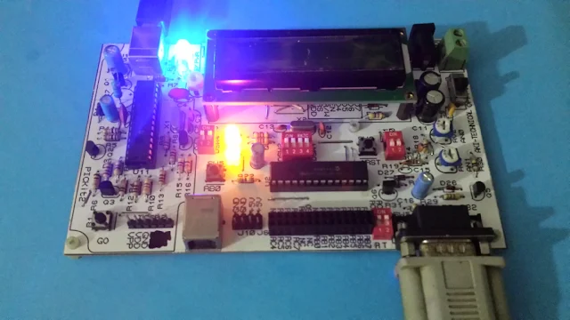
I use MPLABX IDE v1.51 and XC8 compiler v1.35. PICKit2 device programmer/debugger is already plugged in this version of MPLABX version. Programmer can build and run target board using PICKit2 with only one-click. Click here to download this example.

DIY PIC18F2550 USB Board
MPLABX IDE and XC8 Program for LED(s) testing

Search This Blog

Labels

25AA010A (1) 8051 (7) 93AA46B (1) ADC (30) Analog Comparator (1) Arduino (15) ARM (6) AT89C52 (7) ATMega32 (54) AVR (57) CCS PICC (28) DAC (1) DHT11 (2) Display (105) Distance Sensor (3) DS18B20 (3) dsPIC (2) dsPIC30F1010 (2) EEPROM (5) Environment Sensor (4) esp8266 (1) I2C (29) Input/Output (67) Interrupt (19) Keil (5) Keypad (10) LCD (46) Master/Slave (1) MAX7221 (1) MCP23017 (5) MCP23S17 (4) Meter (3) MikroC (2) Motor (15) MPLABX (66) Nokia 5110 LCD (3) OLED (2) One-Wire (6) Oscillator (8) PCB (6) PCD8544 (3) PCF8574 (5) PIC (107) PIC12F (2) PIC16F628A (2) PIC16F630 (1) PIC16F716 (3) PIC16F818 (10) PIC16F818/819 (2) PIC16F84A (15) PIC16F876A (1) PIC16F877A (9) PIC16F88 (1) PIC16F887 (60) PIC18 (19) PIC18F1220 (4) PIC18F2550 (3) PIC18F4550 (12) PWM (11) RTC (8) Sensor (10) SH1106 (1) Shift Register (11) Shift Registers (2) SPI (24) STM32 (6) STM32 Blue Pill (6) STM32CubeIDE (6) STM32F103C8T6 (6) SysTick (3) temperature sensor (11) Thermometer (21) Timer/Counter (30) TM1637 (2) UART (7) Ultrasonic (4) Voltmeter (7) WDT (1) XC16 (2) XC8 (94)