Introduction
PIC18F2550 provides Universal Serial Bus (USB) communication interface, up to 12Mbit/s Full Speed USB 2.0. It can clock up to 48MHz with 12MIPS executing speed using its Phase Lock Loop (PLL) module. This 28-pin USB slave device operates between 2 to 5.5V. Using 5V DC supply voltage allows this chip to operate at its optimal performance.
Unlike Arduino or NXP micro-controllers, this device doesn't come with boot-loader. An external In Circuit System Programmer (ICSP) is needed to burn its firmware into device's internal flash memory. An earlier version of PICKit USB programmer/debugger is a popular low cost device programmer. PICKit2 is very popular due to its price. However it's easy to build for electronics hobbyists. I tried to make this programmer by myself as I was a university student.
Using micro-controller development board would save the prototyping time. However we can assemble a testing board for this micro-controller individually. Assembling device programmer and target testing micro-controller on a single board could be a good way, but it will cost more money and design space.
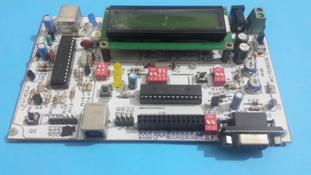 |
| A ready to use prototyping board for PIC18F2550 |
This testing board is already assembled and tested. However it has some fault during the design. I corrected all the on board mistakes and schematic/PCB design.
PCB design and processing
I made schematic and PCB design by myself. Printed circuit was fabricated using a DIY low cost toner transfer method with an in house laser printer. It takes a few days to complete the design, DIY PCB processing, and assembling of all on-board components.
PCB Processing
 |
| Copper clad board with transferred circuit pattern |
 |
| Circuit board after PCB etching |
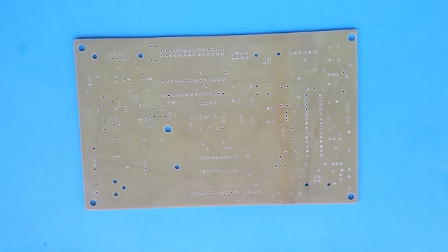 |
| PCB panel after drilling |
It takes around 5 minutes to finish PCB etching. Ferric Chloride is a low cost etching chemical for DIY PCB processing.
 |
| Back panel of PCB |
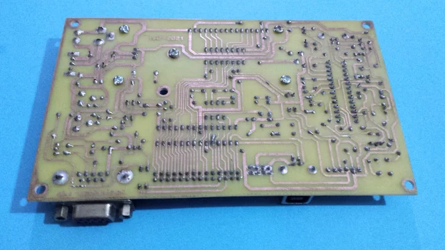 |
| Prototyping board after assembling |
PCB soldering seem to be untidy due to unwell copper track protection during etching. However it doesn't matter for hobbyists.
 |
| Components side after PCB assembling |
Schematic and PCB Design
Schematic design makes up to two design sheet in A4 paper side. One's for PICKit2 device programmer and one's for PIC18F2550 testing board. Schematic for PICKit2 will not be shown here due to its untidiness, but it works.
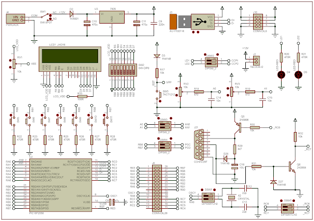 |
| Schematic for testing board |
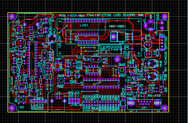 |
| PCB Design View |
I use top copper layer in red color as copper side due to my previous design of PICKit 2 device programmer.
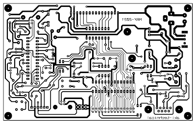 |
| PCB copper side - non-mirror |
It will need some wire jumpers on components side as shown on the picture below.
 |
| Components side and wire jumpers - mirror |
There are some essential blocks on this board:
- PICKit2 device programmer/debugger with external programming header, and DIP switch connects to on-board target PIC device
- Regulated +5V DC supply from external DC voltage input
- Character LCD connects to PortB in 4-bit mode via DIP switch
- Two on-board testing LED(s) connect to RC1 and RC2, enable/disable by DIP switch
- One active low tactile switch connects to RB0 of PortB
- USB connector for USB connection to host computer
- Two trimmer Pots connect to AN0 and AN1, enable/disable by a DIP switch
- RS-232 connector with Tx/Rx pair for UART programming
- PIC18F2550 microcontroller with reset circuit, and a crystal oscillator with a frequency of 20MHz.
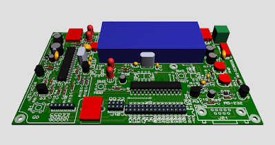 |
| 3D view of PCB design |
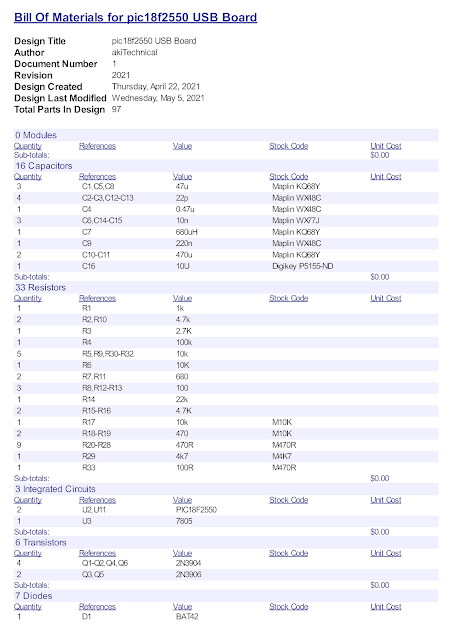
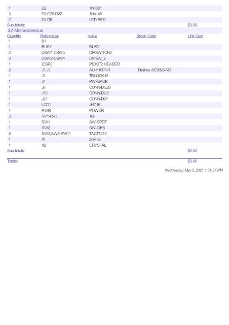
This prototype requires 97 necessary components as it's listed in Bill Of Materials (BOM).
Design file could be download here.
Board and Program Testing
PICKit2 Device Programmer Testing
On this prototyping board, PICKit2 works at +5V DC supplied from USB bus voltage. It works well at fixed +5V voltage.
 |
| This is a screen shot of device programming on Windows 7 x64 host PC while this prototyping board connects onUSB. |
This device programmer is able to power overall system on prototyping board.
Character LCD Test
Character LCD connects to PortB of PIC18F2550 in 4-bit interfacing mode. I test this block using CCS PICC compiler due to its ease of programming.
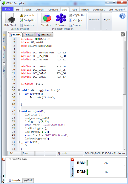 |
| LCD Testing using CCS PICC Program |
The program below is its source code in text format.
#include <18f2550.h>
During device uploading please open SW2 DIP switch, or remove LCD module. DSW4 DIP switch must be closed to enable PGC and PGD of PICKit2 programming header.
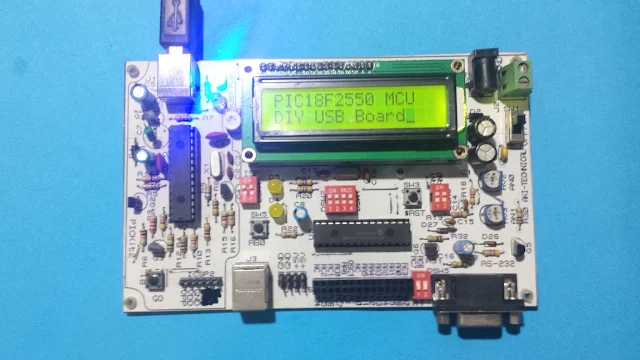 |
| Character LCD testing |
After PICKit2 device uploading please disconnect DSW4, and enable LCD header using SW2.
On-board LED Testing
Two LED(s) connect to RC1 and RC2 of PortC. They are enabled/disabled by DSW2 DIP switch.
XC8 configuration file for PIC18F2550 contain many lines of embedded C directive. I separate this configuration words in one C header file with project folder.
I use MPLABX IDE v1.51 and XC8 compiler v1.35. PICKit2 device programmer/debugger is already plugged in this version of MPLABX version. Programmer can build and run target board using PICKit2 with only one-click. Click here to download this example.
 |
| MPLABX IDE and XC8 Program for LED(s) testing |
A must-have component for anyone building reliable and high-frequency electronic systems—compact, stable, and incredibly efficient in performance.
ReplyDeleteSMD Oscillator
Compact precision meets reliable performance—perfect for today’s high-frequency electronic systems.
ReplyDeleteSurface Mount Oscillator