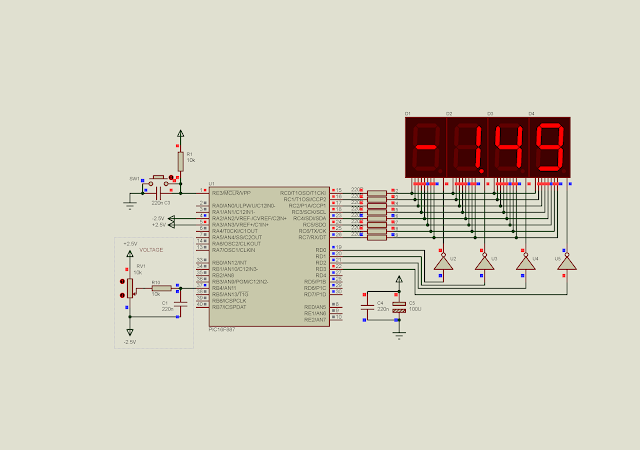
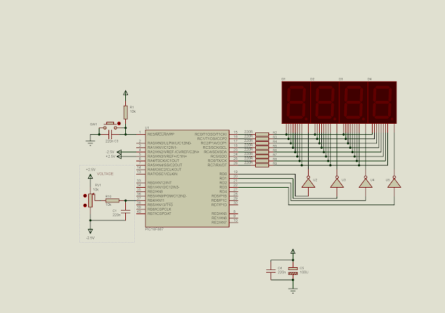
By default two references voltages of the ADC internally connected to VDD and VSS, supplying a +5 V reference voltage for the ADC module. We can change the reference voltage to any value in the total range of +5 V DC.
The VREF+ and VREF- pin could be programmed to externally connect to any voltage reference. By assigning the 'VCFG0' to '1' allows the VREF+ pin connect to external positive voltage. Similarly, by assigning the 'VCFG1' to '1' allows the VREF- pin connect to external negative voltage.
For this example, I connect the VREF+ pin to +2.5 V and the VREF- pin to -2.5 V. Hence, the total reference voltage for the ADC module is,
The step voltage size is 0.00488 V. In this case the the lowest voltage of -2.5 V gives the ADC reading result 0. While the maximum voltage +2.5 V gives the ADC reading result 1023. The zero analog input voltage yields the ADC reading result to 512.
Source code:
#include<xc.h>
// PIC16F887 Configuration Bit Settings
// CONFIG1
#pragma config FOSC = XT
#pragma config WDTE = OFF
#pragma config PWRTE = OFF
#pragma config MCLRE = ON
#pragma config CP = OFF
#pragma config CPD = OFF
#pragma config BOREN = ON
#pragma config IESO = ON
#pragma config FCMEN = ON
#pragma config LVP = ON
// CONFIG2
#pragma config BOR4V = BOR40V
#pragma config WRT = OFF
/*_XTAL_FREQ use for __delay*/
#define _XTAL_FREQ 4000000

void driveDisplays(  int analogRead){
 unsigned char ssd[16]={0x3F,0x06,0x5B,0x4F,0x66,0x6D,0x7D,
 0x07,0x7F,0x6F,0x77,0x7C,0x39,0x5E,0x79,0x71};
 float voltage;
 int _voltage;
 /*Voltage Calculation total reference is
  +5V with centered ground*/
 voltage=(5*((float)(analogRead)/1024))-2.5;
 _voltage=(voltage*100);
 /*Check negative voltage*/
 if(_voltage&0x8000){
     _voltage=-_voltage;
     PORTD=0x00;
 PORTC=0x40;
 PORTD=0x01;
 __delay_ms(10);
 }
 /*Decimal Place*/
 PORTD=0x00;
 PORTC=ssd[_voltage/100]|0x80;
 PORTD=0x02;
 __delay_ms(10);
 /*Floating point*/
 PORTD=0x00;
 PORTC=ssd[(_voltage%100)/10];
 PORTD=0x04;
 __delay_ms(10);
 PORTD=0x00;
 PORTC=ssd[_voltage%10];
 PORTD=0x08;
 __delay_ms(10);
}
int readADC(void){
    GO=1;
    while(GO);
    __delay_ms(10);
    return (ADRESH<<8)+ADRESL;
}
void main(void){
      int adcResult;
    /*Analog and digital Port
     Configuration*/
    PORTB=0x00;
    PORTC=0x00;
    PORTD=0x00;
    /*RB4 for analog input*/
    TRISB4=1;
    TRISC=0x00;
    TRISD=0x00;
    /*Select external Voltage reference
     +2.5V to -2.5V*/
    VCFG1=1;
    VCFG0=1;
    /*Result is right justify*/
    ADFM=1;
    /*By default is analog,
     but again set it to analog*/
    ANS11=1;
    /*Select FRC Clock of ADC module*/
    ADCON0bits.ADCS=0x03;
    /*Turn on ADC Module*/
    ADON=1;
    /*Select AN11 RB4*/
    ADCON0bits.CHS=0x0B;
ADON=1;
/*initiate a conversion*/
GO=1;
/*Wait until GO=0 "done"*/
while(GO);
while(1){
adcResult=readADC();
driveDisplays(adcResult);
}
}
 |
| The screen-shot shows the analog voltage input of -1.49 V. |
Back to main tutorials page.


No comments:
Post a Comment