Overview
The MCP23S17 is an SPI 16-bit (two ports) bi-directional GPIO expansion chip. Its TWI version is the MCP23017. It's rich of functions, data direction, control, distinct input and output registers, programmable weak pull up resistors, interrupt capabilities etc. Its configuration setting is very similar to most of PIC micro-controller since it is produced by Microchip Technology.
 |
| MCP23S17 I/O Ports Programming |
It contains two 8-bit bi-directional port, GPA and GPB. Both of them are programmable with additional interrupt features. Its two interrupt flag pins correspond to each ports.
 |
| MCP23S17-E/SP |
The SPI version of this chip is very similar to the I2C version.
Package Types |
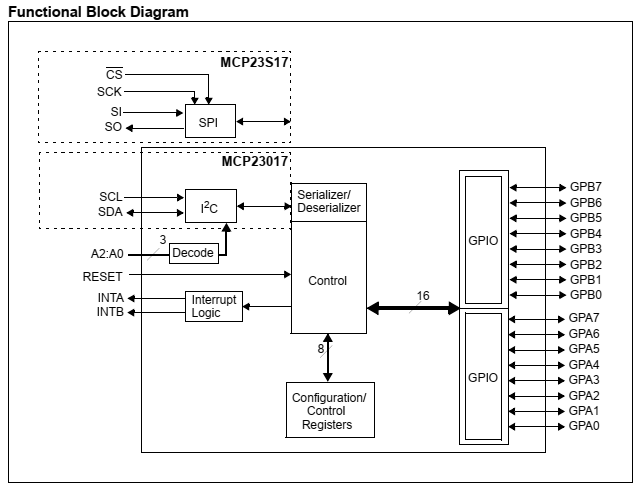
Its SPI interface is bi-directional since it's a general purpose I/O chip. Its four SPI pins are Chip Select(CS), Serial Clock(SCK), Serial In(SI) and Serial Out(SO). Its three optional address pins are A2:A0. We can connect them to GND to set the SPI slave write address to 0x40 and 0x41 for read address.
 |
| Functional Block Diagram |
The programmer must configure the following registers to get a proper operation.
 |
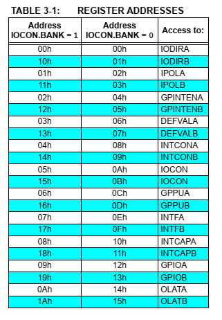
| Register Addressed |
By default we don't set the IOCON register the default bank is BANK0 ranges from 0x00 to 0x15. For example the IODIRB locates at 0x01 and its output register OLATB locates at 0x15.
 |
| SPI ADDRESSING REGISTERS |
The idle state of CS pin is high. To complete a write or read operation the master MCU has to send at least 3 write operations.
ATMega644 and MCP23S17 SPI Programming
The write operations contain three data bytes, slave write address, register address and data. For example to make GPA as output we must do the following step:
- Set CS pin low
- Send its slave address 0x40 (A2:A0=0)
- Send IODIRA address 0x00
- Send data direction 0x00 that is output direction
- Clear CS pin
Here the output ports GPA and GPB are output. They blink LED(s) every half second.
 |
| GPA and GPB are output ports |
 |
| SPI Waveform |
C source Code "main.c":
- /*
- * 12-spi_mcp23s17.c
- *
- * Created: 2/15/2026 9:55:53 PM
- * Author : Admin
- */
- #include <avr/io.h>
- #include <util/delay.h>
- #define F_CPU 16000000UL
- const char MCP23017_W=0x40;
- const char MCP23017_R=0x41;
- //IOCON.BANK=0
- enum BANK0{
- IODIRA=0,IODIRB,IPOLA,IPOLB,GPINTENA,GPINTENB,DEFVALA,
- DEFVALB,INTCONA,INTCONB,IOCON1,IOCON2,GPPUA,GPPUB,
- INTFA,INTFB,INTCAPA,INTCAPB,GPIOA,GPIOB,OLATA,OLATB
- };
- #define DDR_SPI DDRB
- #define PRT_SPI PORTB
- #define DD_MOSI 5
- #define DD_MISO 6
- #define DD_SCK 7
- #define DD_SS 4
- void SPI_MasterInit(void)
- {
- /* Set MOSI and SCK output, all others input */
- DDR_SPI = (1<<DD_MOSI)|(1<<DD_SCK)|(1<<DD_SS);
- /* Enable SPI, Master, set clock rate fck/16 */
- SPCR = (1<<SPE)|(1<<MSTR)|(1<<SPR0);
- }
- void SPI_MasterTransmit(char cData)
- {
- /* Start transmission */
- SPDR = cData;
- /* Wait for transmission complete */
- while(!(SPSR & (1<<SPIF)))
- ;
- }
- void SPI_SlaveInit(void)
- {
- /* Set MISO output, all others input */
- DDR_SPI = (1<<DD_MISO);
- /* Enable SPI */
- SPCR = (1<<SPE);
- }
- char SPI_SlaveReceive(void)
- {
- /* Wait for reception complete */
- while(!(SPSR & (1<<SPIF)))
- ;
- /* Return Data Register */
- return SPDR;
- }
- void mcp23s17_transmit(char address, char data){
- PRT_SPI&=~(1<<DD_SS);
- SPI_MasterTransmit(MCP23017_W);
- SPI_MasterTransmit(address);
- SPI_MasterTransmit(data);
- PRT_SPI|=(1<<DD_SS);
- }
- int main(void)
- {
- /* Replace with your application code */
- SPI_MasterInit();
- PRT_SPI|=(1<<DD_SS); //Set CS Pin High
- // GPA Output
- mcp23s17_transmit(IODIRA,0x00);
- //GPB Output
- mcp23s17_transmit(IODIRB,0x00);
- while (1)
- {
- mcp23s17_transmit(OLATA,0x0F);
- mcp23s17_transmit(OLATB,0x00);
- _delay_ms(500);
- mcp23s17_transmit(OLATA,0xF0);
- mcp23s17_transmit(OLATB,0xFF);
- _delay_ms(500);
- }
- }
At this point the master MCU set a port as input.
This is an example of making GPB as input:
- Set CS pin low
- Send its slave address 0x40 (A2:A0=0)
- Send IODIRB address 0x01
- Send data direction 0xFF that is input direction
- Clear CS pin
And then we enable the weak pull up resistors of GPB:
- Set CS pin low
- Send its slave address 0x40 (A2:A0=0)
- Send GPPUB address 0x0D
- Send 0xFF to turn on all its pull up resistors
- Clear CS pin
The read operation also contains three data bytes, slave read address, register address, any data and read operation. For instance GPB is already an input port. So the MCU needs to read its input data:
- Set CS pin low
- Send its slave address 0x41 (A2:A0=0)
- Send GPIOB address 0x13
- Send one byte of data (eg:0x00) for shift data out from MCP23S17 SO pin
- Perform the SPI read operation
- Clear CS pin
This example GPB of MCP23S17 is an input port with weak pull resistors enabled. The master MCU read data from this port and send it back to GPA output port.
 |
| GPB as Input and GPA as Output |
 |
| Waveform on virtual DSO |
C Source Code "main.c":
- /*
- * 12-spi_mcp23s17_io.c
- *
- * Created: 2/15/2026 10:56:48 PM
- * Author : Admin
- */
- #include <avr/io.h>
- #include <util/delay.h>
- #define F_CPU 16000000UL
- const char MCP23017_W=0x40;
- const char MCP23017_R=0x41;
- //IOCON.BANK=0
- enum BANK0{
- IODIRA=0,IODIRB,IPOLA,IPOLB,GPINTENA,GPINTENB,DEFVALA,
- DEFVALB,INTCONA,INTCONB,IOCON1,IOCON2,GPPUA,GPPUB,
- INTFA,INTFB,INTCAPA,INTCAPB,GPIOA,GPIOB,OLATA,OLATB
- };
- #define DDR_SPI DDRB
- #define PRT_SPI PORTB
- #define DD_MOSI 5
- #define DD_MISO 6
- #define DD_SCK 7
- #define DD_SS 4
- void SPI_MasterInit(void)
- {
- /* Set MOSI and SCK output, all others input */
- DDR_SPI = (1<<DD_MOSI)|(1<<DD_SCK)|(1<<DD_SS);
- /* Enable SPI, Master, set clock rate fck/16 */
- SPCR = (1<<SPE)|(1<<MSTR)|(1<<SPR0);
- }
- void SPI_MasterTransmit(char cData)
- {
- /* Start transmission */
- SPDR = cData;
- /* Wait for transmission complete */
- while(!(SPSR & (1<<SPIF)))
- ;
- }
- void SPI_SlaveInit(void)
- {
- /* Set MISO output, all others input */
- DDR_SPI = (1<<DD_MISO);
- /* Enable SPI */
- SPCR = (1<<SPE);
- }
- char SPI_SlaveReceive(void)
- {
- /* Wait for reception complete */
- while(!(SPSR & (1<<SPIF)))
- ;
- /* Return Data Register */
- return SPDR;
- }
- void mcp23s17_transmit(char address, char data){
- PRT_SPI&=~(1<<DD_SS);
- SPI_MasterTransmit(MCP23017_W);
- SPI_MasterTransmit(address);
- SPI_MasterTransmit(data);
- PRT_SPI|=(1<<DD_SS);
- }
- char mcp23s17_receive(char address){
- PRT_SPI&=~(1<<DD_SS);
- SPI_MasterTransmit(MCP23017_R);
- SPI_MasterTransmit(address);
- SPI_MasterTransmit(0x00);
- char data=SPI_SlaveReceive();
- PRT_SPI|=(1<<DD_SS);
- return data;
- }
- int main(void)
- {
- /* Replace with your application code */
- SPI_MasterInit();
- PRT_SPI|=(1<<DD_SS); //Set CS Pin High
- mcp23s17_transmit(IODIRA,0x00);
- mcp23s17_transmit(IODIRB,0xFF);
- mcp23s17_transmit(GPPUB,0xFF);
- while (1)
- {
- char data=mcp23s17_receive(GPIOB);
- mcp23s17_transmit(OLATA,data);
- _delay_ms(500);
- }
- }
For PIC micro-controller user this post shows how a PIC16F887 interfaces with the MCP23S17 using its dedicated SPI hardware.

No comments:
Post a Comment