Overview
In previous post, I showed about the MSSP module of PIC16F887 with an SPI shift registers example. There are many SPI slave devices, a EEPROM memory, a GPIO extender chip, Flash memory, etc.
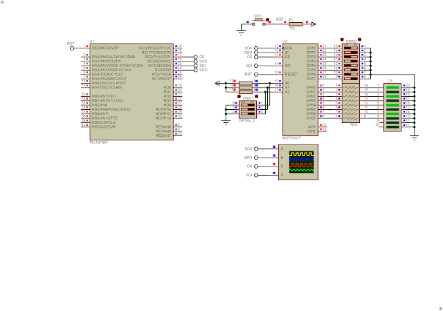 |
| Program Simulation in Proteus |
Here I use a MCP23S17 SPI GPIO expanding chip. The Microchip MCP23X17 series has two options of communication interfaces, the MCP23017 (I2C) and the MCP23S17(SPI). Both of them are bi-directional in data data transaction.
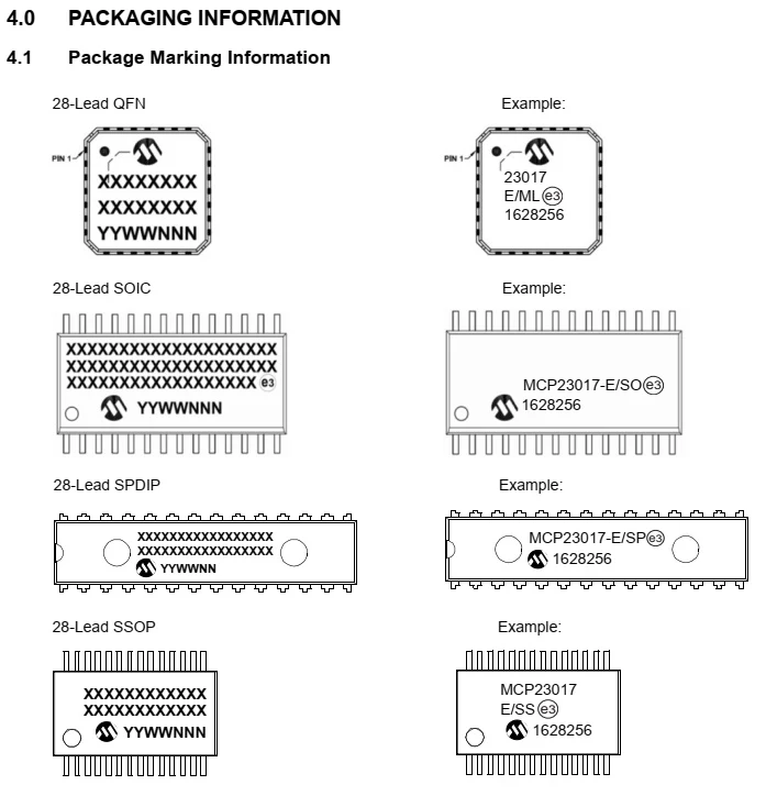 |
| MCP23X17 Packaging Information |
This chip has many package types including the Dual In Line Package (DIP-28) easing the prototyping for electronics hobbyists. I don't have the SPI communication interface of this chip. I have only one MCP23017 I2C one's.
 |
| MCP23017 I2C Type |
This chip can be used for LEDs or relays driving, keypad scanning, LCD driving, etc.
Package Types |
The SPI addressing mode is similar to the I2C mode. It uses a two-byte data package, device address, additional 3-bit addresses, and a read/write bit.
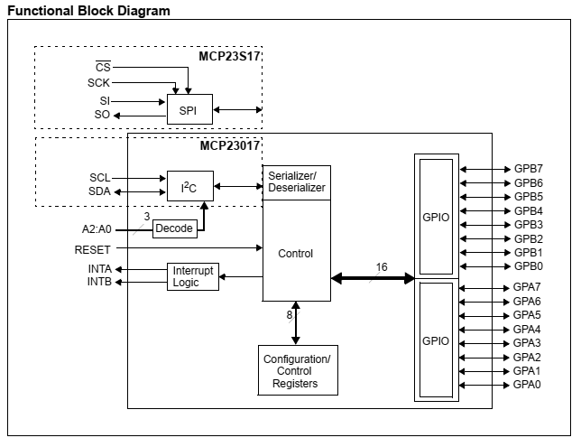 |
| Functional Block Diagram |
For SPI mode (MCP23S17) has the following I/O pins.
- Chip Select (CS) - Active low input signal latching data to its internal registers
- Serial Clock (SCK) - input synchronous clock signal up to 10MHz
- Serial Input (SI) - SPI serial data input (8-bit)
- Serial Output (SO) - SPI serial data output (8-bit)
It has an additional 3-bit addresses (A2:A0). These address could be ignored or enable by software setting. By setting bit 3 of IOCON register we can enable this feature. By default this feature is ignored (A2:A0=0x00) and the memory addressing locates at BANK0 of the registers map.
Reset input (RESET) is active low. This pin can be shared with the micro-controller reset circuit.
GPIOA Interrupt (INTA) and GPIOB Interrupt (INTB) are the output signal notifying the master SPI whenever the input interrupt at GPIOA and GPIOB occurs. However this feature must be enable in its interrupt registers setting.
GPIOA (GPA) and GPIOB (GPB) are digital bi-directional readable/writable ports. Its data direction registers can be selected using the IODIRA and IODIRB registers. These registers will be shown in its registers map.
In SPI mode the clock rate has a maximum frequency of 10MHz.
 |
| SPI Addressing Registers |
Its registers are divide into two banks, BANK0 and BANK1. By default BANK0 is active. So the programmer doesn't need to access BANK1 as it's not necessary.
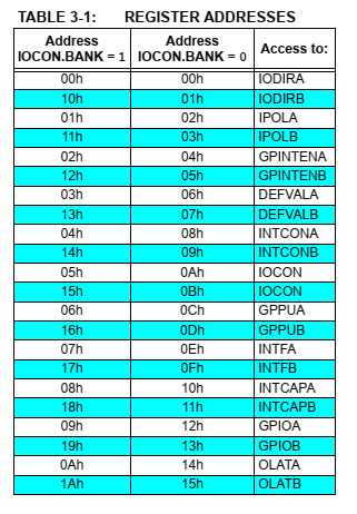 |
| Register Addressed |
For a full details of these registers you can see its device datasheet. Here I will use only some registers to work with.
- IODIRA - I/O DIRECTION REGISTER A (ADDR 0x00) : Clearing its bits for output direction, setting its bits for input direction.
- IODIRB - I/O DIRECTION REGISTER B (ADDR 0x01) : Clearing its bits for output direction, setting its bits for input direction.
- IOCONA - I/O EXPANDER CONFIGURATION REGISTER (ADDR 0x05)
- IOCONB - I/O EXPANDER CONFIGURATION REGISTER (ADDR 0x06)
- GPPUA - GPIO PULL-UP RESISTOR REGISTER A(ADDR 0x0C)
- GPPUB - GPIO PULL-UP RESISTOR REGISTER B(ADDR 0x0D)
- GPIOA - GENERAL PURPOSE I/O PORT REGISTER A (ADDR 0x12)
- GPIOB - GENERAL PURPOSE I/O PORT REGISTER B (ADDR 0x13)
- OLATA - OUTPUT LATCH REGISTER A (ADDR 0x14)
- OLATB - OUTPUT LATCH REGISTER B (ADDR 0x15)
In this example we use use these registers in the MPLABX IDE and XC8 compiler.
PIC16F887 MPLABX IDE and XC8 Programming
I use the high speed SPI communication interface of the MSSP module to interface with this chip. The MCP23S17 SPI slave chip is writable and readable.
GPIOA is configured as digital input reading input data from a DIP switch. GPIOB is configured as digital output writing data to the output LED. I turned on the pull up resistors of GPIOA to raise it high by default.
I created a separate SPI driver in this project.
The SPI.h file:
The SPI.c file:
Click here to download its source file.
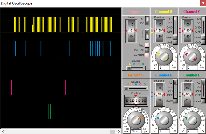 |
| SPI Waveform |
I use a virtual digital oscilloscope to get its waveform.

No comments:
Post a Comment