Overview
The MCP23017 is a 16-bit I2C I/O expander chip. It could be used for digital input reading/writing, relay driving, multiplexing display driving, keypad scanning, LCD controlling, etc. It uses a Two-Wire serial interface or I2C with two communication line, serial data (SDA) and serial clock (SCL).
 |
| Simulating Program for I/O Reading and Writing |
This chip has more functionalities compare to the older PCF8574 I/O expander. It has data direction control, pull-up resistor control, input output register, output latch register, interrupt control and status registers, etc. For an introductory example, you can see this post that I use the ATMega32 micro-controller.
 |
| The MCP23017 DIP-28 I Posses |
This chip comes with various packages. A DIP-28 is preferred for most of electronics hobby projects.
 |
| MCP23017 Package Types |
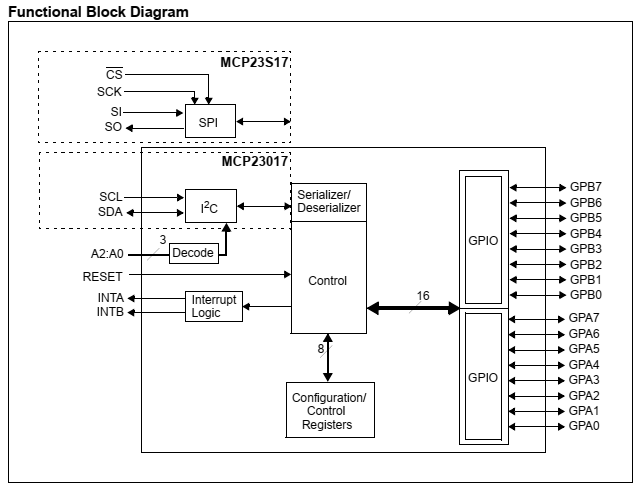
- I2C communication interface
- reset (active high)
- additional address setting
- interrupts output
- two 8-bit bi-directional GPIO, GPA and GPB.
 |
| Functional Block Diagram |
This chip able to operate at high speed up to 1.7MHz. Its operating voltage ranges from 1.8V to 5.5V. For electronics hobbyist prototyping a 5V stable supply voltage is common.
 |
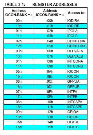
| Register Addresses |
- IODIRA - I/O Direction Register A (0 for output and 1 for input)
- IODIRB - I/O Direction Register B (0 for output and 1 for input)
- GPPUA - GPIO Pull-Up Resistor Register A (1 for enable and 0 for disable)
- GPPUB - GPIO Pull-Up Resistor Register B (1 for enable and 0 for disable)
- GPIOA - General Purpose I/O Port Register A ( this register is for reading data from PORTA)
- GPIOB - General Purpose I/O Port Register B ( this register is for reading data from PORTB)
- OLATA - Output Latch Register A ( this register is for writing data to output PORTA)
- OLATB - Output Latch Register B ( this register is for writing data to output PORTB)
For more detail you can see its datasheet.
To write to this chip the controller needs to write its slave address of 0x40 (A2...A0 are logic 0) followed by its register address and data. It also have sequential addressing mode but I don't mention it here.
To read from this chip the controller needs to write its slave address 0x40 (A2...A0 are logic 0) followed by its register address. Then start a new write session of the device slave address of 0x41 followed the I2C read mode to get the data.
MPLABX IDE and XC8 Programming
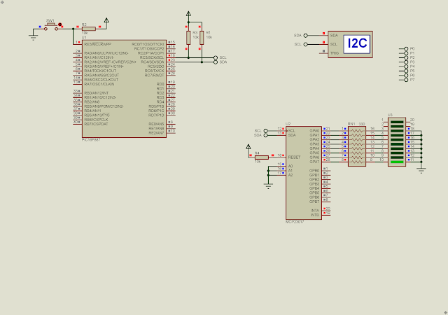
This introductory example, the master micro-processor just send a LED shifting data to the I2C slave MCP23017 chip. I use the I2C communication module of PIC16F887. Its serial clock frequency is 400kHz.
I use only GPA for LED output. The LED shifts for every 100 Milli seconds.
 |
| Proteus Simulation |
The following example, the MCP23017 is used for reading data from GPB and writing data back to GPA.
I enable its pull-up resistor at GPB without adding additional resistor the the circuit.
 |
| Schematic Diagram |
Simulating program in Proteus work very well. Click here to download this example.
No comments:
Post a Comment