Overview
The SNx4HC165 devices are 8-bit parallel-load shift registers that, when clocked, shift the data toward a serial (QH) output. Parallel-in access to each stage is provided by eight individual direct data (A-H) inputs that are enabled by a low level at the shift/load (SH/LD) input. The SNx4HC165 devices also feature a clock-inhibit (CLK INH) function and a complementary serial (QH) output. Clocking is accomplished by a low-to-high transition of the clock (CLK) input while SH/LD is held high and CLK INH is held low. The functions of CLK and CLK INH are interchangeable. Because a low CLK and a low-to-high transition of CLK INH also accomplish clocking, CLK INH must be changed to the high level only while CLK is high. Parallel loading is inhibited when SH/LD is held high. While SH/LD is low, the parallel inputs to the register are enabled independently of the levels of the CLK, CLK INH, or serial (SER) inputs.

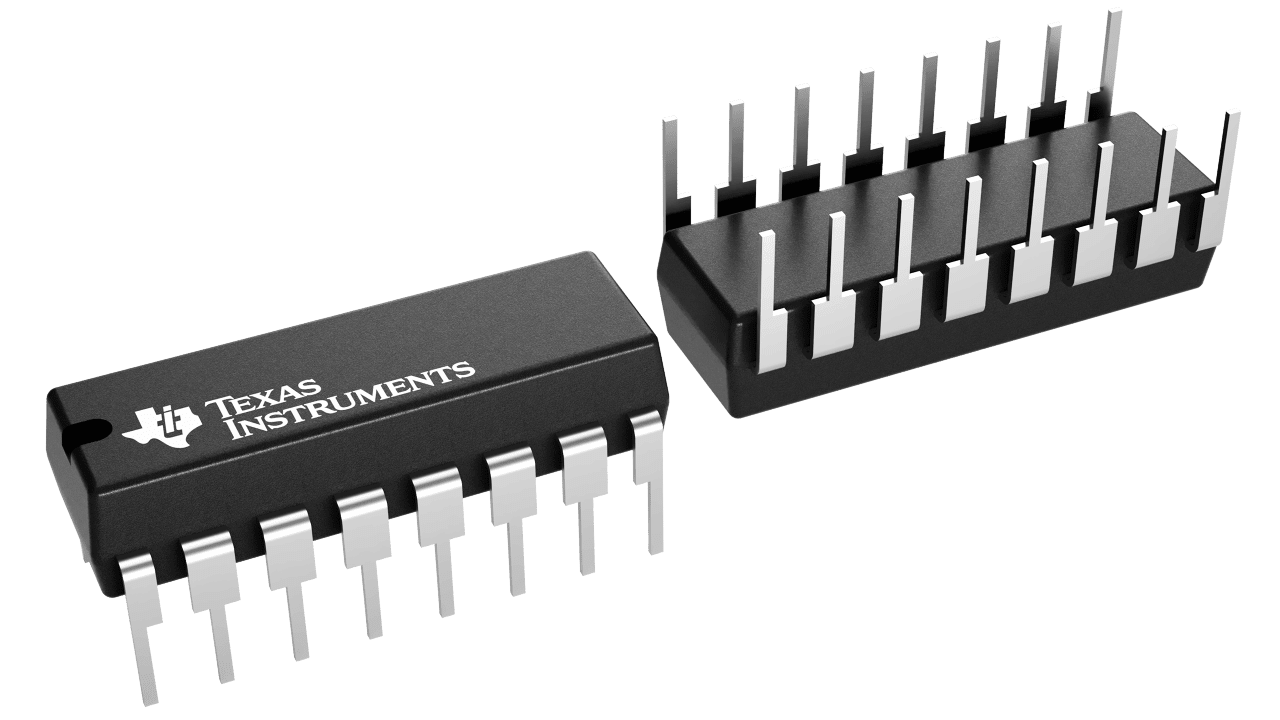
This input expansion chip can be used in Programmable Logic Controllers, Appliances, Video Display Systems, Keyboards etc. This old digital IC is very easy to use with a typical 8-bit MCU since it has a small footprint and its Dual In-Line Package version. It is widely available at very low cost.
 |
| A DIP-16 Sample |
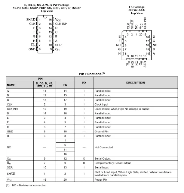
It has DIP-16 footprint and various SMD packages.
 |
| Pin Configuration and Functions |
It made from some digital logic gates and flip-flops.
 |
| Logic Diagram Positive Logic |
To load parallel input data (H:A) take a look at the timing diagram below.
 |
| Load Shift Sequence |
Typically the SI (Serial Data In) is ignored or wires it GND. The Clock Inhabit (CLK INH) must wired to GND. At the transition from logic low to logic high of SH/LD pin allows parallel data loading and serial data shifting out via Serial Data Out (SO) pin.
In this example the ATMega644P read parallel input data of an SN74HC165N and display it on PORTD.
Source Code "main.c":
- /*
- * 12-spi_sn74hc165.c
- *
- * Created: 2/16/2026 11:12:37 AM
- * Author : Admin
- */
- #include <avr/io.h>
- #include <util/delay.h>
- #define F_CPU 16000000UL
- #define DDR_SPI DDRB
- #define PRT_SPI PORTB
- #define DD_SS 4
- #define DD_MOSI 5
- #define DD_MISO 6
- #define DD_SCK 7
- void SPI_MasterInit(void)
- {
- /* Set MOSI and SCK output, all others input */
- DDR_SPI = (1<<DD_MOSI)|(1<<DD_SCK)|(1<<DD_SS);
- /* Enable SPI, Master, set clock rate fck/16 */
- SPCR = (1<<SPE)|(1<<MSTR)|(1<<SPR0);
- }
- void SPI_MasterTransmit(char cData)
- {
- /* Start transmission */
- SPDR = cData;
- /* Wait for transmission complete */
- while(!(SPSR & (1<<SPIF)))
- ;
- }
- void SPI_SlaveInit(void)
- {
- /* Set MISO output, all others input */
- DDR_SPI = (1<<DD_MISO);
- /* Enable SPI */
- SPCR = (1<<SPE);
- }
- char SPI_SlaveReceive(void)
- {
- /* Wait for reception complete */
- while(!(SPSR & (1<<SPIF)))
- ;
- /* Return Data Register */
- return SPDR;
- }
- int main(void)
- {
- /* Replace with your application code */
- SPI_MasterInit();
- //PRT_SPI|=(1<<DD_SS);
- DDRD=0xFF;
- _delay_ms(1000);
- while (1)
- {
- PRT_SPI&=~(1<<DD_SS);
- PRT_SPI|=(1<<DD_SS);
- SPI_MasterTransmit(0x00);
- PORTD=SPI_SlaveReceive();
- _delay_ms(100);
- }
- }
I don't have this chip because local stores don't stock this part. So I can test it only in simulator.

 |
| SPI Transfer and Receive One Byte Of Data Waveform |
We can connect multiple SN74HC165N chips using a daisy-chain configuration. Here I scan two input ports of two SN74HC165N. So the master MCU needs to shift 16 clock cycles (two bytes of data).
 |
| Using Two SN74HC165N chips (Daisy-Chain) |
 |
| SPI Waveform |
Source Code "main.c":
- /*
- * sn74hc165_2.c
- *
- * Created: 2/16/2026 12:49:13 PM
- * Author : Admin
- */
- #include <avr/io.h>
- #include <util/delay.h>
- #define F_CPU 16000000UL
- #define DDR_SPI DDRB
- #define PRT_SPI PORTB
- #define DD_SS 4
- #define DD_MOSI 5
- #define DD_MISO 6
- #define DD_SCK 7
- void SPI_MasterInit(void)
- {
- /* Set MOSI and SCK output, all others input */
- DDR_SPI = (1<<DD_MOSI)|(1<<DD_SCK)|(1<<DD_SS);
- /* Enable SPI, Master, set clock rate fck/16 */
- SPCR = (1<<SPE)|(1<<MSTR)|(1<<SPR0);
- }
- void SPI_MasterTransmit(char cData)
- {
- /* Start transmission */
- SPDR = cData;
- /* Wait for transmission complete */
- while(!(SPSR & (1<<SPIF)))
- ;
- }
- void SPI_SlaveInit(void)
- {
- /* Set MISO output, all others input */
- DDR_SPI = (1<<DD_MISO);
- /* Enable SPI */
- SPCR = (1<<SPE);
- }
- char SPI_SlaveReceive(void)
- {
- /* Wait for reception complete */
- while(!(SPSR & (1<<SPIF)))
- ;
- /* Return Data Register */
- return SPDR;
- }
- int main(void)
- {
- /* Replace with your application code */
- SPI_MasterInit();
- //PRT_SPI|=(1<<DD_SS);
- DDRD=0xFF;
- DDRC=0xFF;
- while (1)
- {
- PRT_SPI&=~(1<<DD_SS);
- PRT_SPI|=(1<<DD_SS);
- SPI_MasterTransmit(0x00);
- PORTD=SPI_SlaveReceive();
- SPI_MasterTransmit(0x00);
- PORTC=SPI_SlaveReceive();
- _delay_ms(100);
- }
- }
For PIC Micro-controller users check this post:
For ATMega32 AVR micro-controller user check this post:
No comments:
Post a Comment