728x90

Sunday, August 15, 2021

Introduction to A/D Converter Module of PIC16F818

Introduction

An analog input module inside a microcontroller adds an additional function for the controller to convert external analog data from outside world. For example a variable analog input voltage, temperature data converted by a thermometer, pressure, etc.

This module convert analog input data into a digital presentation that digital controller (microcontroller) able to work with. Most of PIC microcontroller comes with Analog-to-Digital (A/D) converter peripheral. A/D conversion resolution is between 8-bit and 10-bit depends on the device. Resolution of an A/D converter refers to its conversion result.

A/D Converter Module of PIC16F818

Analog-to-Digital converter module of PIC16F818 has 10-bit resolution. Its conversion result ranges from 0 to 1023 (1024 in total). Two reference voltage pins are – AVSS and AVDD. These two pins are programmable to connect to internal supply voltage rail or externally connect to user-defined reference voltage sources.

Introduction to A/D Converter Module of PIC16F818
Analog-to-Digital converter block diagram 

A/D Converter Module Registers

There are four basic registers that control and monitor the operation of A/D converter module.

  • A/D Result High Register (ADRESH)
  • A/D Result Low Register (ADRESL)
  • A/D Control Register 0 (ADCON0)
  • A/D Control Register 1 (ADCON1)

A/D Control Register 0 (ADCON0) locates at 1Fh in SFR. It contains A/D clock source selection, channel selection, start of conversion switch, and module’s on/off.

Introduction to A/D Converter Module of PIC16F818
A/D Control Register 0 (ADCON0) 

A/D Control Register 1 (ADCON1) locates at address 9Fh.

Introduction to A/D Converter Module of PIC16F818
A/D Control Register 1 (ADCON1) 

This register contains,

  • A/D Result Format Select bit
  • A/D Clock Divide by 2 Select bit
  • A/D Port Configuration Control bit.

ADRESH and ADRESL are 8-bit register pair to make a 10-bit A/D conversion result.

A/D Converter Input Channels

PIC16F818-I/P in DIP package has five analog input channel, RA0/AN0 to RA4/AN4. To use it as an analog input channel its port data direction control (TRISA) must be set to input direction.

Introduction to A/D Converter Module of PIC16F818
A/D Converter Input Channels 

Bit 3 to 0 of ADCON1 is called A/D Port Configuration Control (PCFG<3:0) bits. It configures between analog and digital I/O pin and reference voltage selection.

AD-Port-Configuration-Register-of-ADCON0
A/D Port Configuration Control (PCFG<3:0) bits of ADCON1

We will talk about reference voltage selection at the next section.

Analog input channel selection must is done using the Analog Channel Select bits (CHS2:CHS0) of ADCON0. This setting must be done first before starting the A/D conversion.

Introduction to A/D Converter Module of PIC16F818
Analog Channel Select bits (CHS2:CHS0) 

To change the input channel for conversion the program must update these bits.

A/D Conversion Clock Source

Clock source for A/D converter module has two inputs – microcontroller clock and internal A/D module RC oscillator. A/D Conversion Clock Select bits (ADCS1:ADCS0) of ADCON0 choose between these two clock sources.

Introduction to A/D Converter Module of PIC16F818
A/D Conversion Clock Select bits (ADCS1:ADCS0) of ADCON0 

Another bit ADCS2 locates in ADCON1. It can force the A/D clock source to drive from microcontroller clock with a frequency of FOSC/2.

Using the A/D module RC oscillator the conversion takes between 2 to 6us.

Turning On and Start of A/D Conversion

Bit 0 of ADCON0 is A/D On (ADON) bit that turn on and off the A/D converter module. Setting it to turn on this module.

Bit 2 of ADCON0 is called A/D Conversion Status (GO/nDONE) bit. Setting this bit to make a conversion. Testing (reading) this bit to poll for conversion result.

Reference Voltage Pins

AVSS and AVDD are the microcontroller internal reference voltage pins. They are the total supply voltage to microcontroller.

VREF- and VREF+ are the A/D converter reference voltage pins. These two pins are programmable to connect between microcontroller AVSS/AVDD pins or externally connected to outside voltage source.

Reference voltage pins are configured in A/D Port Configuration Control (PCFG<3:0) bits of ADCON1 register. To make job done easily the user must configure the module to internally connect its reference voltage pins to microcontroller supply pins – AVSS and AVDD.

Reference voltage effects the A/D module step voltage.

A/D Result Format

Ten-bit result can be arranged in two way – left and right justified. It’s configured in bit 7 – A/D Result Format Select (ADFM) bit of ADCON1 register.

Introduction to A/D Converter Module of PIC16F818
A/D Result Justification 

Setting ADFM to justify the A/D result in right hand, otherwise in left hand.

A/D Converter Programming Example

We have discussed on some basic details on A/D converter module of PIC16F818. Now let make a programming example of this module.

Hardware Preparation

As it’s shown in the schematic below, PIC16F818 drives from its internal 8MHz oscillator that will be configured in program.

Introduction to A/D Converter Module of PIC16F818
Schematic Diagram 

External reset circuit is added in this example. RA0/AN0 is an analog input pin reading analog input voltage from POT. RB7 is a digital output pin connects to a green LED.

Whenever the analog reading exceed 512 digital value it turn on RB7.

Program Preparation

XC8 program configure this controller to clock from its internal oscillator. A/D converter module clock source is its internal A/D oscillator that selected in program.

/*
 * A/D converter example of PIC16F818
 * programming using MPLABX XC8
 */

#include <xc.h>

// PIC16F818 Configuration Bit Settings

// CONFIG
#pragma config FOSC = INTOSCIO  // Oscillator Selection bits (INTRC oscillator; port I/O function on both RA6/OSC2/CLKO pin and RA7/OSC1/CLKI pin)
#pragma config WDTE = OFF       // Watchdog Timer Enable bit (WDT disabled)
#pragma config PWRTE = OFF      // Power-up Timer Enable bit (PWRT disabled)
#pragma config MCLRE = ON       // RA5/MCLR/VPP Pin Function Select bit (RA5/MCLR/VPP pin function is MCLR)
#pragma config BOREN = ON       // Brown-out Reset Enable bit (BOR enabled)
#pragma config LVP = OFF         // Low-Voltage Programming Enable bit (RB3/PGM pin has PGM function, Low-Voltage Programming enabled)
#pragma config CPD = OFF        // Data EE Memory Code Protection bit (Code protection off)
#pragma config WRT = OFF        // Flash Program Memory Write Enable bits (Write protection off)
#pragma config CCPMX = RB2      // CCP1 Pin Selection bit (CCP1 function on RB2)
#pragma config CP = OFF         // Flash Program Memory Code Protection bit (Code protection off)

void main(void){   
    /*Select 8MHz internal oscillator*/
    OSCCONbits.IRCF=0x07;
    /*Clear Port A*/
    PORTA=0x00;
    /*Clear Port B*/
    PORTB=0x00;
    /*RA0 analog input*/
    TRISA=0x01;
    /*Port B digital output*/
    TRISB=0x00;
    /*Select internal RC oscillator of A/D converter*/
    ADCON0bits.ADCS=0x01;
    /*Select analog channel 0 - AN0*/
    ADCON0bits.CHS=0x00;
    /*RA0-AN0 analog input, AVDD and AVSS voltage references*/
    ADCON1bits.PCFG=14;
    /*Result is right justified*/
    ADCON1bits.ADFM=1;
    /*Turn on A/D converter module*/
    ADCON0bits.ADON=1;
    /*Main Program Loop*/
    while(1){
        /*Start the conversion*/
        ADCON0bits.GO_nDONE=1;
        /*When GO_nDONE is clear A/D conversion is completed*/
        while(GO_nDONE);
        /*Wait for some microseconds*/
        for(int i=0;i<1000;i++);
        /*Make a 10-bit A/D converter result*/
        int _L=ADRESL;
        int _H=ADRESH;
        int result = (_H<<8)+_L;
        /*If analog voltage is more than half RB4 is set*/
        RB7 = (result>=512)?1:0;
    }
}

Total source code of this example program looks very long. Currently most of new microcontroller programmer prefers Arduino as a reason of ready-to-use hardware, rich of libraries, and shortness of codes. Click here to download zip file of this example program.


Saturday, August 14, 2021

Programming the External Interrupt of PIC16F818 in XC8


Introduction

In microcontroller, interrupt is hardware or software event notification to the system. Each time interrupt occurs the system could respond or ignore to that event. Amount of interrupt capabilities of microcontroller is different. Interrupt triggered by internal or external events.

Programming the External Interrupt of PIC16F818 in XC8
Simulation Sample of this programming example


PIC16F818 has many interrupt sources that we can not list them all here. External interrupt is an interrupt source triggered by external logic change on pin RB0 of port B in PIC16F818/819. It can be an interrupt on falling or rising edge depends on user configuration in software.

External Interrupt Preparation

There are many steps of software configuration in programming. We will need to configure port data direction, interrupt edge, global interrupt control, etc.

Port Data Direction

Pin RB0 must be a digital input as it’s a logic input to the microcontroller. An optional weak pull-up resistor could save the number of external add-on components and circuit wiring. Hence the user must clear nRBPU of the OPTION register.

Programming the External Interrupt of PIC16F818 in XC8
OPTION Register

But the interrupt edge must selected to work in falling edge of input logic.

Interrupt Edge Selection

Edge of external interrupt are rising and falling edge. The user select between these two mode using Interrupt Edge Select Bit (INTEDG) of the OPTION register.

Programming the External Interrupt of PIC16F818 in XC8
Interrupt Edge Select Bit

Clearing this bit to select the interrupt on falling edge from external input device – for example a motion sensor.

Turning on External Interrupt

Interrupt Control Register (INTCON) consists of many interrupt source setting and interrupt flag, including the external interrupt. An interrupt flag in PIC microcontroller is set whenever the corresponding interrupt source occurs. The user must test and clear this flag in software at the time it occurs and ended.

Programming the External Interrupt of PIC16F818 in XC8
Interrupt Control Register (INTCON)

Bit 7 of INTCON is a Global Interrupt Enable bit (GIE) is a general interrupt switch. Setting to ‘1’ before other interrupt sources are enabled.

Bit 4 is an External Interrupt Enable bit (INTE). Setting this bit to turn on external interrupt on RB0.

Bit 1 is an External Interrupt Flag bit (INTF). This bit must be cleared first in the first program configuration for the external interrupt. In the Interrupt Service Routine (ISR), the code must test this bit to find its occurrence.

Interrupt Service Routine

An Interrupt Service Routine (ISR) is a piece of code written in the interrupt vector of PIC microcontroller. It responses to the interrupt whenever it’s enabled an occured.

In mid-range PIC microcontroller as PIC16F818 there is only one interrupt vector locates at the address 0x04 in program memory. However in a high level programming language like XC8 we don’t care about this vector. ISR in XC8 is just a C function but it’s reserved for interrupt vector.

void interrupt _ISR_NAME(void){
//Code here
}

In ISR the user must test the interrupt flag, writing codes to response to interrupt, and clear interrupt flag.

XC8 Programming for External Interrupt

This simple external interrupt programming example show a blinking LED as its normal main program routine. Whenever the external interrupt occurs, it toggles an output LED.

Schematic Diagram

External interrupt attaches to RB0 while two output LED are the main program loop blinking and another LED is interrupt response.

Programming the External Interrupt of PIC16F818 in XC8
Schematic diagram for this interrupt programming example

SW2 triggers the external interrupt at whenever it’s pressed.

XC8 Programming

Software setting configure this controller to use its internal oscillator clocks at 4MHz. Other remaining code are written to support the interrupt capabilities.

/*PIC16F818 External Interrupt Example
 * Using MPLABX XC8
 */
#include <xc.h>

// PIC16F818 Configuration Bit Settings
// CONFIG
#pragma config FOSC = INTOSCIO  // Oscillator Selection bits (INTRC oscillator; port I/O function on both RA6/OSC2/CLKO pin and RA7/OSC1/CLKI pin)
#pragma config WDTE = OFF       // Watchdog Timer Enable bit (WDT disabled)
#pragma config PWRTE = OFF      // Power-up Timer Enable bit (PWRT disabled)
#pragma config MCLRE = OFF      // RA5/MCLR/VPP Pin Function Select bit (RA5/MCLR/VPP pin function is digital I/O, MCLR internally tied to VDD)
#pragma config BOREN = ON       // Brown-out Reset Enable bit (BOR enabled)
#pragma config LVP = OFF        // Low-Voltage Programming Enable bit (RB3/PGM pin has digital I/O function, HV on MCLR must be used for programming)
#pragma config CPD = OFF        // Data EE Memory Code Protection bit (Code protection off)
#pragma config WRT = OFF        // Flash Program Memory Write Enable bits (Write protection off)
#pragma config CCPMX = RB2      // CCP1 Pin Selection bit (CCP1 function on RB2)
#pragma config CP = OFF         // Flash Program Memory Code Protection bit (Code protection off)

#define _XTAL_FREQ 1000000

/*Naming the Output LED*/
#define toggleLed   RB7
#define blinkLed    RB6

void main(void){
    /*Oscillator Setup 1MHz*/
    OSCCONbits.IRCF=0x04;
    /*Clear Port B*/
    PORTB=0x00;
    /*RB0 Input */
    TRISB=0x01;
    /*Turn On Pull Up Resistor*/
    nRBPU=0;
    /*Enable Global Interrupt*/
    GIE=1;
    /*Enable External Interrupt*/
    INTE=1;
    /*Select Interrupt on Falling Edge*/
    INTEDG=0;
    /*Clear Interrupt Flag*/
    INTF=0;
    while(1){
        blinkLed^=1;
        __delay_ms(250);
    }
}

void interrupt _ISR(void){
  /*Test external interrupt flag*/
    if(INTF){
      /*Clear flag*/
        INTF=0;
      /*Toggle LED*/
        toggleLed^=1;
    }
}

Click here to download this example archive.

Thursday, August 12, 2021

Programming Timer0 of PIC16F818 in XC8


Introduction

Timer of a microcontroller is an auto-incremental register configured by user’s program. It’s useful for creating a timing delay, measuring the duration of external event, etc.

Programming Timer0 of PIC16F818 in XC8
A software simulation sample of this programming example


Timer0 of PIC16F818

Timer0 is an 8-bit read/write register locates at the address 01h and 101h in SFR. Timer0 works in both timer and counter mode, but we mention only timer mode in this post.

Programming Timer0 of PIC16F818 in XC8
Block Diagram of Timer0/WDT Prescaler

This peripheral module contains its storage register TMR0, control registers and its interrupt flag.

Prescaler Selection

Both timer and counter mode have a programmable prescaler, as it’s configured in Option register (OPTION_REG).

Programming Timer0 of PIC16F818 in XC8
OPTION_REG of PIC16F818

Its 8-bit Prescaler must between Timer0 and Watch Dog Timer (WDT) prescaler. These two prescaler selection is set in Prescaler Assignment bit (PSA). Setting PSA assigns its prescaler to the WDT, otherwise it’s assigned to Timer0 module.

Prescaler Rate Select bits (PS2:0) of the OPTION_REG configures the prescaler between 1:1 and 1:256.

Programming Timer0 of PIC16F818 in XC8
Prescaler Rate Select bits (PS2:0)

To get a 1:1 prescaler it must switch to WDT Rate. But getting a 1:256 prescaler rate it must switch to TMR0 Rate as listed above.

Timer0 Overflow and Interrupt

Timer0 register TMR0 is an 8-bit wide register. As it’s configured to a free running register that clocks from the microcontroller instruction clock, it triggers an interrupt flag at the time it reaches 0xFF (255 in decimal) and rolls back to 0. This interrupt flag is called Timer0 Overflow Interrupt Flag (TMR0IF), locates in the INTCON.

Programming Timer0 of PIC16F818 in XC8
Timer0 Overflow Interrupt Flag (TMR0IF) of INTCON

User’s program must clear this flag in code. This flag is auto-set whenever the overflow happens regardless of Timer0 Interrupt Enable bit (TMR0IE). We will show about timer 0 interrupt programming in later post.

Timer0 Programming in XC8

We have mentioned about timer utilization in microcontroller. Now we will use this microcontroller inside’s to create a timing delay of about one second. This one second pulse blink the LED.

Circuit Design

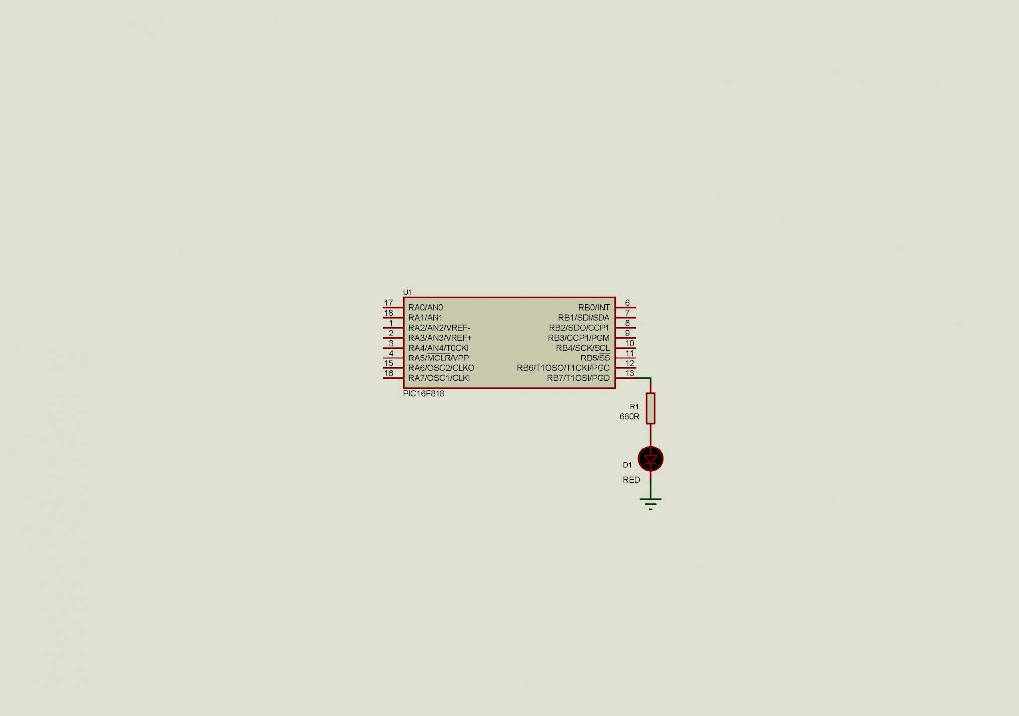
Microcontroller system circuit is very simple. It’s just build with a +5V power supply unit and its output LED connects to RB7. We don’t need microcontroller reset circuit and crystal oscillator.

Programming Timer0 of PIC16F818 in XC8
Circuit diagram without reset and clock circuit

Calculation for Timer 0 Overflow

With its feature of internal RC oscillator, the system select its 8MHz maximum clock frequency to heart-beat the CPU. For Mid-Range PIC device its instruction rate is,

Fosc/4 = 8MHz/4 = 2MHz or 2MIPS , as its instruction executing time is mostly completed in only one instruction cycle.

The cycle time of its instruction clock is,

1/(2MHz) = 0.5us.

I choose the 1:256 prescaler. So timer 0 clock input has a rate of.

256*0.5us = 128us.

Eight-bit TMR0 register overflows and set its interrupt flag within this duration,

256*128us = 32.768ms.

To find an approximate 1 second delay,

1/(32.768ms) = 30.51 counts or 31 counts.

All setting will be set and shown in programming section next time.

XC8 Programming

XC8 program set the controller to utilize its 8MHz maximum clock frequency as it’s done with OSCCON register. Option register configure timer 0 mode of operation to work as a free running counter with a prescaler of 1:256.

The program main loop regularly test the interrupt flag (TMR0IF). As it’s set a C variable will increase by 1, until it reaches a one second count. The the time of getting its one second count, RB7 toggles its output LED.

Its C program made of between 40 and 50 lines of code.

/*
 */
#include <xc.h>
// PIC16F818 Configuration Bit Settings
// CONFIG
#pragma config FOSC = INTOSCIO  // Oscillator Selection bits (INTRC oscillator; port I/O function on both RA6/OSC2/CLKO pin and RA7/OSC1/CLKI pin)
#pragma config WDTE = OFF       // Watchdog Timer Enable bit (WDT disabled)
#pragma config PWRTE = OFF      // Power-up Timer Enable bit (PWRT disabled)
#pragma config MCLRE = OFF      // RA5/MCLR/VPP Pin Function Select bit (RA5/MCLR/VPP pin function is digital I/O, MCLR internally tied to VDD)
#pragma config BOREN = ON       // Brown-out Reset Enable bit (BOR enabled)
#pragma config LVP = OFF        // Low-Voltage Programming Enable bit (RB3/PGM pin has digital I/O function, HV on MCLR must be used for programming)
#pragma config CPD = OFF        // Data EE Memory Code Protection bit (Code protection off)
#pragma config WRT = OFF        // Flash Program Memory Write Enable bits (Write protection off)
#pragma config CCPMX = RB2      // CCP1 Pin Selection bit (CCP1 function on RB2)
#pragma config CP = OFF         // Flash Program Memory Code Protection bit (Code protection off)
#define onSecondCounts  31
void main(void){
    unsigned int intCounts=0;
    /*Select 8MHz Crystal Frequency*/
    OSCCONbits.IRCF=0x07;
    /*Clear Port B*/
    PORTB=0x00;
    /*RB7 digital output*/
    TRISB&=~(1<<7);
    /*Select internal MCU clock for Timer0*/
    T0CS=0;
    /*Select Timer 0 Prescaler*/
    PSA=0;
    /*Select 1:256 Prescaler*/
    OPTION_REGbits.PS=0x07;
    /*Clear timer 0 overflow interrupt flag*/
    TMR0IF=0;
    /*Clear Timer 0*/
    TMR0=0;
    while(1){
        if(TMR0IF){
            TMR0IF=0;
            intCounts+=1;
        }
        if(intCounts>=onSecondCounts){
            intCounts=0;
            RB7^=1;
        }
    }
}

Generated hex file requires only 4.7% of the total program memory space.

Program Testing

Both software simulation and physical hardware experiment work in the same manner. However in Proteus simulator the delay time is shorter than in physical hardware experiment.

Programming Timer0 of PIC16F818 in XC8
microcontroller program experiment on breadboard

I don’t show the picture of Proteus simulation here due its duplication. Click here to download this example in zip file format.


Search This Blog