Introduction
An analog input module inside a microcontroller adds an additional function for the controller to convert external analog data from outside world. For example a variable analog input voltage, temperature data converted by a thermometer, pressure, etc.
This module convert analog input data into a digital presentation that digital controller (microcontroller) able to work with. Most of PIC microcontroller comes with Analog-to-Digital (A/D) converter peripheral. A/D conversion resolution is between 8-bit and 10-bit depends on the device. Resolution of an A/D converter refers to its conversion result.
A/D Converter Module of PIC16F818
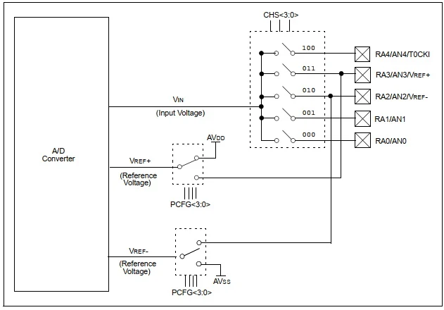
Analog-to-Digital converter module of PIC16F818 has 10-bit resolution. Its conversion result ranges from 0 to 1023 (1024 in total). Two reference voltage pins are – AVSS and AVDD. These two pins are programmable to connect to internal supply voltage rail or externally connect to user-defined reference voltage sources.
 |
| Analog-to-Digital converter block diagram |
A/D Converter Module Registers
There are four basic registers that control and monitor the operation of A/D converter module.
- A/D Result High Register (ADRESH)
- A/D Result Low Register (ADRESL)
- A/D Control Register 0 (ADCON0)
- A/D Control Register 1 (ADCON1)
A/D Control Register 0 (ADCON0) locates at 1Fh in SFR. It contains A/D clock source selection, channel selection, start of conversion switch, and module’s on/off.
 |
| A/D Control Register 0 (ADCON0) |
A/D Control Register 1 (ADCON1) locates at address 9Fh.
 |
| A/D Control Register 1 (ADCON1) |
This register contains,
- A/D Result Format Select bit
- A/D Clock Divide by 2 Select bit
- A/D Port Configuration Control bit.
ADRESH and ADRESL are 8-bit register pair to make a 10-bit A/D conversion result.
A/D Converter Input Channels
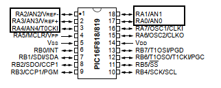
PIC16F818-I/P in DIP package has five analog input channel, RA0/AN0 to RA4/AN4. To use it as an analog input channel its port data direction control (TRISA) must be set to input direction.
 |
| A/D Converter Input Channels |
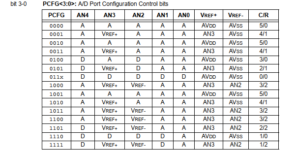
Bit 3 to 0 of ADCON1 is called A/D Port Configuration Control (PCFG<3:0) bits. It configures between analog and digital I/O pin and reference voltage selection.
 |
| A/D Port Configuration Control (PCFG<3:0) bits of ADCON1 |
We will talk about reference voltage selection at the next section.
Analog input channel selection must is done using the Analog Channel Select bits (CHS2:CHS0) of ADCON0. This setting must be done first before starting the A/D conversion.
 |
| Analog Channel Select bits (CHS2:CHS0) |
To change the input channel for conversion the program must update these bits.
A/D Conversion Clock Source
Clock source for A/D converter module has two inputs – microcontroller clock and internal A/D module RC oscillator. A/D Conversion Clock Select bits (ADCS1:ADCS0) of ADCON0 choose between these two clock sources.
 |
| A/D Conversion Clock Select bits (ADCS1:ADCS0) of ADCON0 |
Another bit ADCS2 locates in ADCON1. It can force the A/D clock source to drive from microcontroller clock with a frequency of FOSC/2.
Using the A/D module RC oscillator the conversion takes between 2 to 6us.
Turning On and Start of A/D Conversion
Bit 0 of ADCON0 is A/D On (ADON) bit that turn on and off the A/D converter module. Setting it to turn on this module.
Bit 2 of ADCON0 is called A/D Conversion Status (GO/nDONE) bit. Setting this bit to make a conversion. Testing (reading) this bit to poll for conversion result.
Reference Voltage Pins
AVSS and AVDD are the microcontroller internal reference voltage pins. They are the total supply voltage to microcontroller.
VREF- and VREF+ are the A/D converter reference voltage pins. These two pins are programmable to connect between microcontroller AVSS/AVDD pins or externally connected to outside voltage source.
Reference voltage pins are configured in A/D Port Configuration Control (PCFG<3:0) bits of ADCON1 register. To make job done easily the user must configure the module to internally connect its reference voltage pins to microcontroller supply pins – AVSS and AVDD.
Reference voltage effects the A/D module step voltage.
A/D Result Format
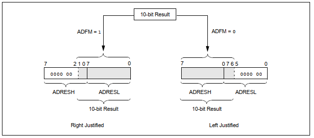
Ten-bit result can be arranged in two way – left and right justified. It’s configured in bit 7 – A/D Result Format Select (ADFM) bit of ADCON1 register.
 |
| A/D Result Justification |
Setting ADFM to justify the A/D result in right hand, otherwise in left hand.
A/D Converter Programming Example
We have discussed on some basic details on A/D converter module of PIC16F818. Now let make a programming example of this module.
Hardware Preparation
As it’s shown in the schematic below, PIC16F818 drives from its internal 8MHz oscillator that will be configured in program.
 |
| Schematic Diagram |
External reset circuit is added in this example. RA0/AN0 is an analog input pin reading analog input voltage from POT. RB7 is a digital output pin connects to a green LED.
Whenever the analog reading exceed 512 digital value it turn on RB7.
Program Preparation
XC8 program configure this controller to clock from its internal oscillator. A/D converter module clock source is its internal A/D oscillator that selected in program.
/*
 * A/D converter example of PIC16F818
 * programming using MPLABX XC8
 */

#include <xc.h>

// PIC16F818 Configuration Bit Settings

// CONFIG
#pragma config FOSC = INTOSCIO  // Oscillator Selection bits (INTRC oscillator; port I/O function on both RA6/OSC2/CLKO pin and RA7/OSC1/CLKI pin)
#pragma config WDTE = OFF       // Watchdog Timer Enable bit (WDT disabled)
#pragma config PWRTE = OFF      // Power-up Timer Enable bit (PWRT disabled)
#pragma config MCLRE = ON       // RA5/MCLR/VPP Pin Function Select bit (RA5/MCLR/VPP pin function is MCLR)
#pragma config BOREN = ON       // Brown-out Reset Enable bit (BOR enabled)
#pragma config LVP = OFF         // Low-Voltage Programming Enable bit (RB3/PGM pin has PGM function, Low-Voltage Programming enabled)
#pragma config CPD = OFF        // Data EE Memory Code Protection bit (Code protection off)
#pragma config WRT = OFF        // Flash Program Memory Write Enable bits (Write protection off)
#pragma config CCPMX = RB2      // CCP1 Pin Selection bit (CCP1 function on RB2)
#pragma config CP = OFF         // Flash Program Memory Code Protection bit (Code protection off)

void main(void){
    /*Select 8MHz internal oscillator*/
    OSCCONbits.IRCF=0x07;
    /*Clear Port A*/
    PORTA=0x00;
    /*Clear Port B*/
    PORTB=0x00;
    /*RA0 analog input*/
    TRISA=0x01;
    /*Port B digital output*/
    TRISB=0x00;
    /*Select internal RC oscillator of A/D converter*/
    ADCON0bits.ADCS=0x01;
    /*Select analog channel 0 - AN0*/
    ADCON0bits.CHS=0x00;
    /*RA0-AN0 analog input, AVDD and AVSS voltage references*/
    ADCON1bits.PCFG=14;
    /*Result is right justified*/
    ADCON1bits.ADFM=1;
    /*Turn on A/D converter module*/
    ADCON0bits.ADON=1;
    /*Main Program Loop*/
    while(1){
        /*Start the conversion*/
        ADCON0bits.GO_nDONE=1;
        /*When GO_nDONE is clear A/D conversion is completed*/
        while(GO_nDONE);
        /*Wait for some microseconds*/
        for(int i=0;i<1000;i++);
        /*Make a 10-bit A/D converter result*/
        int _L=ADRESL;
        int _H=ADRESH;
        int result = (_H<<8)+_L;
        /*If analog voltage is more than half RB4 is set*/
        RB7 = (result>=512)?1:0;
    }
}
Total source code of this example program looks very long. Currently most of new microcontroller programmer prefers Arduino as a reason of ready-to-use hardware, rich of libraries, and shortness of codes. Click here to download zip file of this example program.
No comments:
Post a Comment