Introduction
Timer of a microcontroller is an auto-incremental register configured by user’s program. It’s useful for creating a timing delay, measuring the duration of external event, etc.
 |
| A software simulation sample of this programming example |
Timer0 of PIC16F818
Timer0 is an 8-bit read/write register locates at the address 01h and 101h in SFR. Timer0 works in both timer and counter mode, but we mention only timer mode in this post.
 |
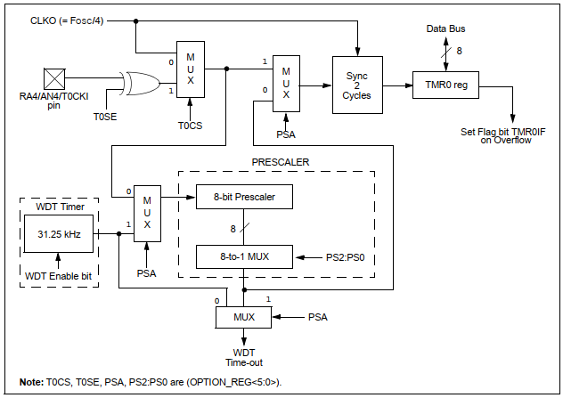
| Block Diagram of Timer0/WDT Prescaler |
This peripheral module contains its storage register TMR0, control registers and its interrupt flag.
Prescaler Selection
Both timer and counter mode have a programmable prescaler, as it’s configured in Option register (OPTION_REG).
 |
| OPTION_REG of PIC16F818 |
Its 8-bit Prescaler must between Timer0 and Watch Dog Timer (WDT) prescaler. These two prescaler selection is set in Prescaler Assignment bit (PSA). Setting PSA assigns its prescaler to the WDT, otherwise it’s assigned to Timer0 module.
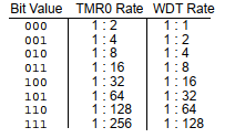
Prescaler Rate Select bits (PS2:0) of the OPTION_REG configures the prescaler between 1:1 and 1:256.
 |
| Prescaler Rate Select bits (PS2:0) |
To get a 1:1 prescaler it must switch to WDT Rate. But getting a 1:256 prescaler rate it must switch to TMR0 Rate as listed above.
Timer0 Overflow and Interrupt
Timer0 register TMR0 is an 8-bit wide register. As it’s configured to a free running register that clocks from the microcontroller instruction clock, it triggers an interrupt flag at the time it reaches 0xFF (255 in decimal) and rolls back to 0. This interrupt flag is called Timer0 Overflow Interrupt Flag (TMR0IF), locates in the INTCON.
 |
| Timer0 Overflow Interrupt Flag (TMR0IF) of INTCON |
User’s program must clear this flag in code. This flag is auto-set whenever the overflow happens regardless of Timer0 Interrupt Enable bit (TMR0IE). We will show about timer 0 interrupt programming in later post.
Timer0 Programming in XC8
We have mentioned about timer utilization in microcontroller. Now we will use this microcontroller inside’s to create a timing delay of about one second. This one second pulse blink the LED.
Circuit Design
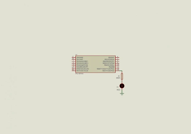
Microcontroller system circuit is very simple. It’s just build with a +5V power supply unit and its output LED connects to RB7. We don’t need microcontroller reset circuit and crystal oscillator.
 |
| Circuit diagram without reset and clock circuit |
Calculation for Timer 0 Overflow
With its feature of internal RC oscillator, the system select its 8MHz maximum clock frequency to heart-beat the CPU. For Mid-Range PIC device its instruction rate is,
Fosc/4 = 8MHz/4 = 2MHz or 2MIPS , as its instruction executing time is mostly completed in only one instruction cycle.
The cycle time of its instruction clock is,
1/(2MHz) = 0.5us.
I choose the 1:256 prescaler. So timer 0 clock input has a rate of.
256*0.5us = 128us.
Eight-bit TMR0 register overflows and set its interrupt flag within this duration,
256*128us = 32.768ms.
To find an approximate 1 second delay,
1/(32.768ms) = 30.51 counts or 31 counts.
All setting will be set and shown in programming section next time.
XC8 Programming
XC8 program set the controller to utilize its 8MHz maximum clock frequency as it’s done with OSCCON register. Option register configure timer 0 mode of operation to work as a free running counter with a prescaler of 1:256.
The program main loop regularly test the interrupt flag (TMR0IF). As it’s set a C variable will increase by 1, until it reaches a one second count. The the time of getting its one second count, RB7 toggles its output LED.
Its C program made of between 40 and 50 lines of code.
*/
#include <xc.h>
// PIC16F818 Configuration Bit Settings
// CONFIG
#pragma config FOSC = INTOSCIO // Oscillator Selection bits (INTRC oscillator; port I/O function on both RA6/OSC2/CLKO pin and RA7/OSC1/CLKI pin)
#pragma config WDTE = OFF // Watchdog Timer Enable bit (WDT disabled)
#pragma config PWRTE = OFF // Power-up Timer Enable bit (PWRT disabled)
#pragma config MCLRE = OFF // RA5/MCLR/VPP Pin Function Select bit (RA5/MCLR/VPP pin function is digital I/O, MCLR internally tied to VDD)
#pragma config BOREN = ON // Brown-out Reset Enable bit (BOR enabled)
#pragma config LVP = OFF // Low-Voltage Programming Enable bit (RB3/PGM pin has digital I/O function, HV on MCLR must be used for programming)
#pragma config CPD = OFF // Data EE Memory Code Protection bit (Code protection off)
#pragma config WRT = OFF // Flash Program Memory Write Enable bits (Write protection off)
#pragma config CCPMX = RB2 // CCP1 Pin Selection bit (CCP1 function on RB2)
#pragma config CP = OFF // Flash Program Memory Code Protection bit (Code protection off)
#define onSecondCounts 31
void main(void){
unsigned int intCounts=0;
/*Select 8MHz Crystal Frequency*/
OSCCONbits.IRCF=0x07;
/*Clear Port B*/
PORTB=0x00;
/*RB7 digital output*/
TRISB&=~(1<<7);
/*Select internal MCU clock for Timer0*/
T0CS=0;
/*Select Timer 0 Prescaler*/
PSA=0;
/*Select 1:256 Prescaler*/
OPTION_REGbits.PS=0x07;
/*Clear timer 0 overflow interrupt flag*/
TMR0IF=0;
/*Clear Timer 0*/
TMR0=0;
while(1){
if(TMR0IF){
TMR0IF=0;
intCounts+=1;
}
if(intCounts>=onSecondCounts){
intCounts=0;
RB7^=1;
}
}
}
Generated hex file requires only 4.7% of the total program memory space.
Program Testing
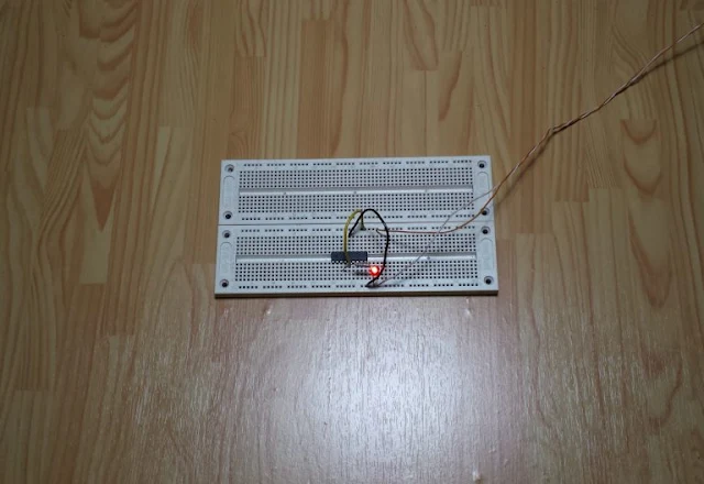
Both software simulation and physical hardware experiment work in the same manner. However in Proteus simulator the delay time is shorter than in physical hardware experiment.
 |
| microcontroller program experiment on breadboard |
I don’t show the picture of Proteus simulation here due its duplication. Click here to download this example in zip file format.
No comments:
Post a Comment