Learn To Write Code For 8051, Arduino, AVR, dsPIC, PIC, STM32 ARM Microcontroller, etc.
Coding Embedded Controller With C/C++.
Printed Circuit Board (PCB) Project For Electronics Hobbyists.
As it’s discussed in previous post, Timer0 of PIC microcontroller is able to trigger an interrupt signal every time its timer register overflows and reset to its initial value of 0.
Programming for Timer0 interrupt is just like other interrupt programming for PIC microcontroller in MPLABX XC8. The programmer is required to enable its global interrupt switch, Timer0 interrupt enable bit, writing an interrupt service routine, etc.
Timer0 Interrupt Programming
We have discussed a lot in previous post about a preparation for interrupt in XC8 programming. Special function registers relate to this interrupt are already shown in these posts.
More About Related Registers
Option register (OPTION_REG) is in used for selecting clock source, timer mode and its clock prescaler.
OPTION Register – OPTION_REG
Interrupt Control Register (INTCON) contain some fundamental interrupt control bits and flags.
Interrupt Control Register – INTCON
Set Global Interrupt Enable (GIE) bit to enable interrupt for any interrupt source.
Timer0 Overflow Interrupt Enable (TMR0IE) bit must be set to turn on timer 0 interrupt capability.
Timer0 Overflow Interrupt Flag (TMR0IF) bit functions as a testing flag to find the present of timer 0 overflow interrupt occurrence. Initially the program must clear this flag and Timer0 register (TMR0) in software.
Circuit Diagram for Hooking Up and Simulation
The system is prepared to utilize an external crystal oscillator with its maximum frequency of 20MHz. It’s optionally have a reset circuit as usual micro-controllers have. We can ignore this reset circuit in configuration section in source code as it was done in previous post.
Circuit diagram for both physical hardware prototyping and software simulation
XC8 Programming
Since the system clock is 20MHz we will need to find all related timing parameters to predict the interrupt interval.
Instruction executing speed is a quarter of microcontroller clock source. So the microcontroller speed is,
FOSC = (20MHz/4) = 5MHz or 5MIPS.
Instruction executing frequency is.
(1/5MHz) = 0.2us.
Timer0 prescaler is 1:256 then Timer0 input clock rate is,
(256*0.2us)= 51.2us.
Timer0 overflow interrupt occurs for every,
(256*51.2us) = 13.1ms.
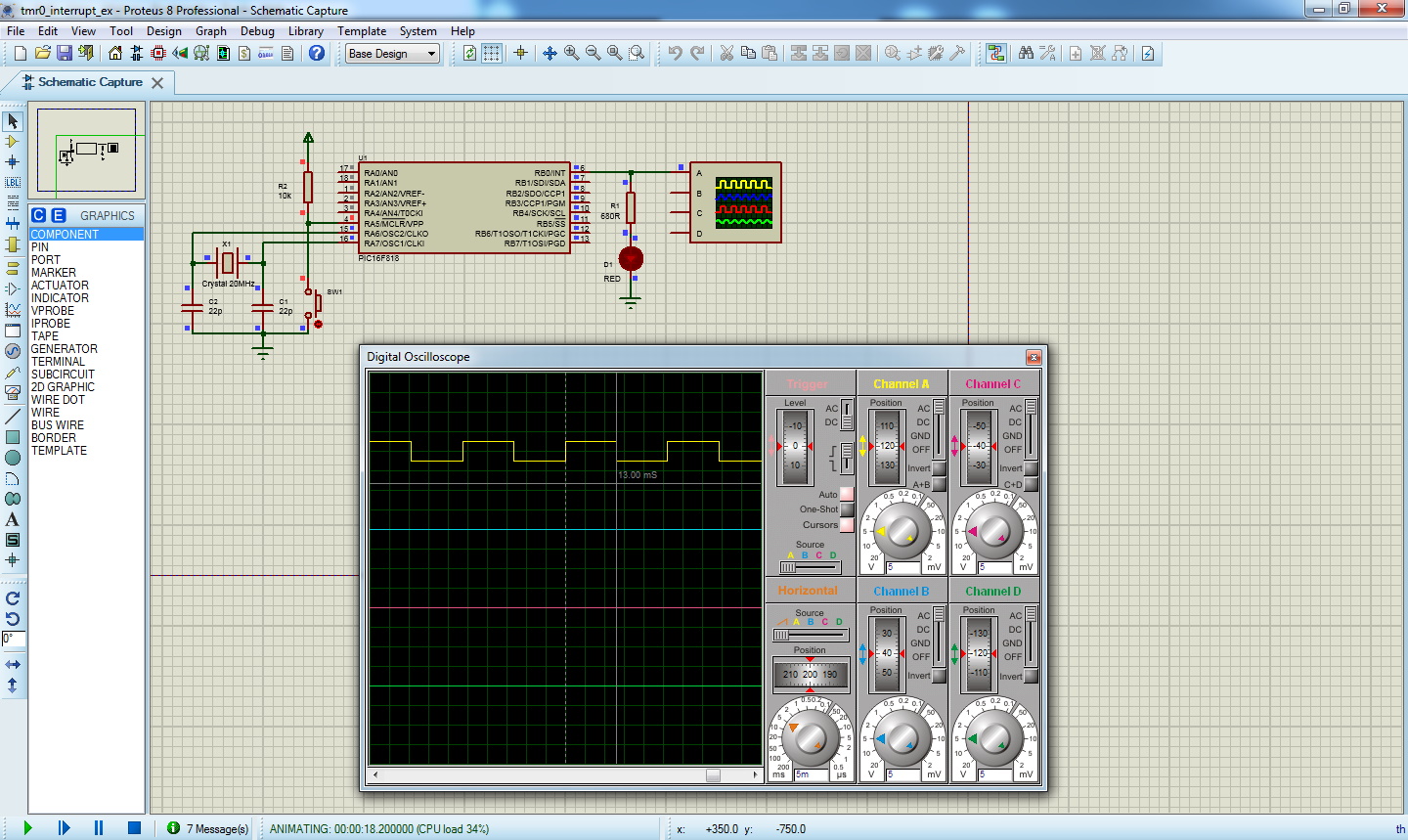
Finally for every 13.1ms, RB0 of PIC16F818 changes its output logic state.
/* * PIC16F818 Timer0 Interrupt * Programming Example */ #include <xc.h> // PIC16F818 Configuration Bit Settings // CONFIG #pragma config FOSC = HS // Oscillator Selection bits (HS oscillator) #pragma config WDTE = OFF // Watchdog Timer Enable bit (WDT disabled) #pragma config PWRTE = OFF // Power-up Timer Enable bit (PWRT disabled) #pragma config MCLRE = ON // RA5/MCLR/VPP Pin Function Select bit (RA5/MCLR/VPP pin function is MCLR) #pragma config BOREN = ON // Brown-out Reset Enable bit (BOR enabled) #pragma config LVP = ON // Low-Voltage Programming Enable bit (RB3/PGM pin has PGM function, Low-Voltage Programming enabled) #pragma config CPD = OFF // Data EE Memory Code Protection bit (Code protection off) #pragma config WRT = OFF // Flash Program Memory Write Enable bits (Write protection off) #pragma config CCPMX = RB2 // CCP1 Pin Selection bit (CCP1 function on RB2) #pragma config CP = OFF // Flash Program Memory Code Protection bit (Code protection off) void main(void){ /*Clear Port B*/ PORTB=0x00; /*Port B As Digital Output*/ TRISB=0x00; /*Select Timer0 Prescaler*/ PSA=0; /*Select timer mode*/ T0CS=0; /*Select 1:256 Prescaler*/ OPTION_REGbits.PS=0x07; /*Enable Global Interrupt*/ GIE=1; /*Enable Timer0 Overflow Interrupt*/ TMR0IE=1; /*Clear Timer0 register*/ TMR0=0; /*Clear Timer0 Overflow Interrupt Flag*/ TMR0IF=0; /*Main program loop contain void of codes*/ while(1); } void interrupt timer0ISR(void){ /*Check for Timer0 overflow*/ if(TMR0IF){ /*Clear overflow flag*/ TMR0IF=0; RB0^=1; } }
Simulation in Proteus
There is no essence to prototype this programming example on a real bared board. However it will require an oscilloscope to keep track of output signal on RB0 pin. I just see the result of this programming in simulator. Click here to download this example in zip file format.
Port B of PIC16F818/819 is an 8-bit wide bi-directional digital I/O port. It’s input/output direction is controlled by its data direction register TRISB. Optionally it has an internal weak pull up resistors individually connects to each pin of Port B. However this 8 resistor network is programmable on/off by software.
Pin Diagram of PIC16F818 from device’s datasheet
Port Data and Its Direction Control
Port B locates at 06h and 106h in the Special Function Register (SFR). It’s bi-directional read/write.
Port B Data Direction Register (TRISB) locates at 86h and 186h. Writing ‘1’ to any bit of this register forcing that bit to an input pin, otherwise forcing that bit to an output pin.
Internal Weak Pull Up Resistor
Port B is programmable connect to an internal weak pull up resistors network. There is only one global switch that turn this resistor network on and off. It it’s the PORTB Pull-up Enable bit (nRBPU), of the OPTION register (OPTION_REG) locates at 81h and 181h.
Option Register of PIC16F818
This bit locates at bit 7. Clearing it to enable the internal weak pull up resistor.
Internal Weak Pull Up Resistor Programming in XC8
Using this free version of embedded C compiler, the overall coding is done within a light afford. A simple example shows how to use this feature of PIC microcontroller without adding external resistors to the digital input.
Schematic Diagram
This schematic diagram uses in both physical hardware wiring and software simulation.
Schematic diagram drawn in Proteus
RB0 connects to SW2 to turn of the LED D2 whenever it’s pressed. SW1 connects to SW1 to turn off the LED D2 whenever it’s pressed. It’s clock source is an internal oscillator inside the device with a frequency of 31.25kHz.
XC8 Programming
Embedded C program prepare the internal oscillator, I/O direction, and turning on its internal weak pull up resistor.
/* XC8 Program to use PIC16F818 * internal weak pull up resistor */ #include <xc.h> // PIC16F818 Configuration Bit Settings // CONFIG #pragma config FOSC = INTOSCIO // Oscillator Selection bits (INTRC oscillator; port I/O function on both RA6/OSC2/CLKO pin and RA7/OSC1/CLKI pin) #pragma config WDTE = OFF // Watchdog Timer Enable bit (WDT disabled) #pragma config PWRTE = OFF // Power-up Timer Enable bit (PWRT disabled) #pragma config MCLRE = OFF // RA5/MCLR/VPP Pin Function Select bit (RA5/MCLR/VPP pin function is digital I/O, MCLR internally tied to VDD) #pragma config BOREN = ON // Brown-out Reset Enable bit (BOR enabled) #pragma config LVP = OFF // Low-Voltage Programming Enable bit (RB3/PGM pin has digital I/O function, HV on MCLR must be used for programming) #pragma config CPD = OFF // Data EE Memory Code Protection bit (Code protection off) #pragma config WRT = OFF // Flash Program Memory Write Enable bits (Write protection off) #pragma config CCPMX = RB2 // CCP1 Pin Selection bit (CCP1 function on RB2) #pragma config CP = OFF // Flash Program Memory Code Protection bit (Code protection off) /*Label the inputs outputs*/ #define _ON RB0==0 #define _OFF RB1==0 #define _LED1 RB7 void main(void){ /*Set internal oscillator to 31.25kHz*/ OSCCONbits.IOFS=0x00; /*Clear Port B*/ PORTB=0x00; /*RB0.1 Digital Input*/ TRISB=0x03; /*Turn On Pull Up Resistors*/ OPTION_REGbits.nRBPU=0; /*Main Program Loop*/ while(1){ if(_ON){ while(_ON); _LED1=1; } if(_OFF){ while(_OFF); _LED1=0; } } }
This program requires only 2.4% of program memory (Flash).
Simulator and Physical Hardware Testing
Both simulator and external physical hardware testing produce the same result.
PIC16F818/19 comes with 8 types of oscillator from Low Power (LP) crystal to ECIO. Device’s specification sheet lists all its types below.
Oscillator Types of PIC16F818/19
From that list we have see two options of internal oscillator – INTIO1 and INTIO2. With INTIO2 we can access its internal oscillator with an advantage of getting two full I/O control on RA6 and RA7 pins.
An old used PIC16F818-I/P I stock in my own DIY lab.
Using this feature we can save components requirement at the time of physical hardware prototyping. The two clock pins – RA6 and RA7 can be used as a digital I/O. Furthermore, this internal Resistor/Capacitor (RC) oscillator is precise than the external crystal. As it’s placed internally it can withstand from noisy environment.
Clock diagram of PIC16F818/19
However it has a maximum frequency of 8MHz. PIC16F818/19 can operate up to its maximum external crystal oscillator of the frequency 20MHz. This highest frequency is useful for some applications.
Getting Ready for Programming and Interfacing
XC8 C compiler that run in its MPLABX IDE is a preferred embedded C compiler for PIC microcontroller. I have been using it many years now.
This programming example, I configure the embedded program to access the internal oscillator of PIC16F818 to its maximum frequency of 8MHz. The embedded program is just blinking an output LED connects to RA7.
Setting Up the Device
First we need to prototype this example program in software simulator for safety reason. The circuit diagram below is drawn using Proteus VSM.
Circuit diagram for simulation and hardware prototyping
Pin 14 is VDD pin while pin 5 is for the GND. These pins are hidden and it’s internally connected to both supply pin in this simulator.
Programming in MPLABX XC8
There are some register setting in C source code to configure this device properly. They are,
Configuration Word
Oscillator Tuning Register (OSCTUNE)
Oscillator Control Register (OSCCON)
Configuration Word
Oscillator Selection bits of the Configuration Word allows the user to select between some types of micro-controller’s oscillator.
Configuration Register of PIC16F818/819 (Address 2007h)
We will need to set FOSC2:FOSC0 to “100” in binary to select the internal oscillator inside the controller, and I/O function on its two clock pins.
Oscillator Selection bits
However in MPLABX XC8 C compiler we don’t need to access Configuration Word directly. It’s just done using the #pragma config directive.
pragma config FOSC = INTOSCIO
We can get these codes from the Configuration bits Source Window in MPLABX IDE.
Oscillator Tuning Register – OSCTUNE
This register allows the controller to fine tune to any frequency between 31.25kHz and its maximum 8MHz frequency. However we rarely use this register setting.
In this tutorial we don’t need to use this register. We work with the Internal Oscillator Frequency Select bits of this register only.
Programming in XC8
This programming tutorial is very simple. The main program just configure the internal oscillator with a frequency of 8MHz, and repeatedly toggle an output LED on RA7 with a rate of one second.
/* * File: main.c * Author: admin * * Created on December 16, 2020, 6:45 PM */ #include <stdio.h> #include <stdlib.h> #include <xc.h> // PIC16F818 Configuration Bit Settings // CONFIG #pragma config FOSC = INTOSCIO // Oscillator Selection bits (INTRC oscillator; port I/O function on both RA6/OSC2/CLKO pin and RA7/OSC1/CLKI pin) #pragma config WDTE = OFF // Watchdog Timer Enable bit (WDT disabled) #pragma config PWRTE = OFF // Power-up Timer Enable bit (PWRT disabled) #pragma config MCLRE = ON // RA5/MCLR/VPP Pin Function Select bit (RA5/MCLR/VPP pin function is MCLR) #pragma config BOREN = ON // Brown-out Reset Enable bit (BOR enabled) #pragma config LVP = OFF // Low-Voltage Programming Enable bit (RB3/PGM pin has digital I/O function, HV on MCLR must be used for programming) #pragma config CPD = OFF // Data EE Memory Code Protection bit (Code protection off) #pragma config WRT = OFF // Flash Program Memory Write Enable bits (Write protection off) #pragma config CCPMX = RB2 // CCP1 Pin Selection bit (CCP1 function on RB2) #pragma config CP = OFF // Flash Program Memory Code Protection bit (Code protection off) #define _XTAL_FREQ 8000000 int main(int argc, char** argv) { /*Use its maximum 8MHz Internal Oscillator*/ OSCCONbits.IRCF=0x07; /*Clear Port A*/ PORTA=0x00; /*RA7 output*/ TRISAbits.TRISA7=0; /*Main Loop*/ while(1){ /*Toggling RA7*/ RA7^=1; __delay_ms(1000); } return (EXIT_SUCCESS); }
Getting the Result
There is no differences between software simulator and real physical hardware testing of this programming tutorial. Click here to download source file.
Circuit diagram and simulation result from Proteus VSM
RA7 regularly blinks its output green LED. Red LED connects to RB0 turned on a moment after the microcontroller powered on.
It’s the same to one’s in simulator testing. LED connects to RB0 indicate the stability of the internal oscillator. It wait for a while to turn on after the controller started up.
Oscillator Stability
Program Preparation
INTOSC Frequency Stable bit (bit 2) of OSCCON register indicates the stability of internal oscillator. It’s set whenever the operation of oscillator is stable.
bit 2 – IOFS : INTOSC Frequency Stable bit
Now let test the stability solidity of this oscillator with an XC8 example. RB0 of Port B connects to an red LED via a current limiting resistor, specify the stability of internal oscillator. Logic value of RB0 is no other than the IOFS bit of the OSCCON register.
/* An XC8 Program to test the * INTOSC Frequency Stability */ #include <xc.h> // PIC16F818 Configuration Bit Settings // CONFIG #pragma config FOSC = INTOSCIO // Oscillator Selection bits (INTRC oscillator; port I/O function on both RA6/OSC2/CLKO pin and RA7/OSC1/CLKI pin) #pragma config WDTE = OFF // Watchdog Timer Enable bit (WDT disabled) #pragma config PWRTE = OFF // Power-up Timer Enable bit (PWRT disabled) #pragma config MCLRE = ON // RA5/MCLR/VPP Pin Function Select bit (RA5/MCLR/VPP pin function is MCLR) #pragma config BOREN = ON // Brown-out Reset Enable bit (BOR enabled) #pragma config LVP = OFF // Low-Voltage Programming Enable bit (RB3/PGM pin has digital I/O function, HV on MCLR must be used for programming) #pragma config CPD = OFF // Data EE Memory Code Protection bit (Code protection off) #pragma config WRT = OFF // Flash Program Memory Write Enable bits (Write protection off) #pragma config CCPMX = RB2 // CCP1 Pin Selection bit (CCP1 function on RB2) #pragma config CP = OFF // Flash Program Memory Code Protection bit (Code protection off) #define _XTAL_FREQ 8000000 void main(void) { /*Use its maximum 8MHz Internal Oscillator*/ OSCCONbits.IRCF=0x07; /*Clear Port B*/ PORTB=0x00; /*RB0 Output To LED*/ TRISBbits.TRISB0=0; /*Clear Port A*/ PORTA=0x00; /*RA7 output*/ TRISAbits.TRISA7=0; /*Main Loop*/ while(1){ /*Toggling RA7*/ RA7^=1; __delay_ms(1000); /*RB0 is high whenever the the oscillator is stable*/ RB0=IOFS; } }
We are going to test this embedded program in either simulator and physical hardware.
Getting the Result
Primarily this embedded programming example was tested using Proteus VSM simulator. The circuit diagram preparation has an additional component – the LED connects to RB0.
Circuit diagram and simulation result from Proteus VSM
RA7 regularly blinks its output green LED. Red LED connects to RB0 turned on a moment after the microcontroller powered on.
Hardware test on breadboard
It’s the same to one’s in simulator testing. LED connects to RB0 indicate the stability of the internal oscillator. It wait for a while to turn on after the controller started up. Click here to download source file.
Using Clock Pin As a Digital Input
Using the INTOSCIO configuration, both RA6 and RA7 is digital I/O controlled by its Tri-State register.
An input button connects to RA6 is an active signal. Whenever it’s pressed, the program waits until it’s released, and toggle an output LED connects to RA7.
Circuit diagram and simulation in software
D2 LED connects to RB0 monitor the stability of the controller’s internal oscillator.
Physical hardware test of Using Clock Pin As a Digital Input
Hardware testing produced a similar result to the simulator. XC8 program comes with additional codes that continuously check the input logic state of push button.
/*
Internal oscillator example
* with digital input
*/
#include <xc.h>
// PIC16F818 Configuration Bit Settings
// CONFIG
#pragma config FOSC = INTOSCIO // Oscillator Selection bits (INTRC oscillator; port I/O function on both RA6/OSC2/CLKO pin and RA7/OSC1/CLKI pin)
#pragma config WDTE = OFF // Watchdog Timer Enable bit (WDT disabled)
#pragma config PWRTE = OFF // Power-up Timer Enable bit (PWRT disabled)
#pragma config MCLRE = ON // RA5/MCLR/VPP Pin Function Select bit (RA5/MCLR/VPP pin function is MCLR)
#pragma config BOREN = ON // Brown-out Reset Enable bit (BOR enabled)
#pragma config LVP = OFF // Low-Voltage Programming Enable bit (RB3/PGM pin has digital I/O function, HV on MCLR must be used for programming)
#pragma config CPD = OFF // Data EE Memory Code Protection bit (Code protection off)
#pragma config WRT = OFF // Flash Program Memory Write Enable bits (Write protection off)
#pragma config CCPMX = RB2 // CCP1 Pin Selection bit (CCP1 function on RB2)
#pragma config CP = OFF // Flash Program Memory Code Protection bit (Code protection off)