Learn To Write Code For 8051, Arduino, AVR, dsPIC, PIC, STM32 ARM Microcontroller, etc.
Coding Embedded Controller With C/C++.
Printed Circuit Board (PCB) Project For Electronics Hobbyists.
As we can see in the previous post, the analog input channels could be selected by the CHS bits of the ADCON0 register.
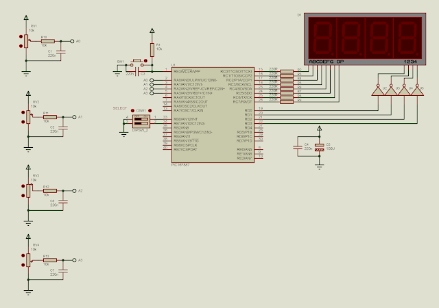
In this example I use the ADC module to read four input analog pins RA0, RA1, RA2 and RA3. The selection is made by A 2 positions DIP switch. This DIP switch could make four values. This value make the selection of analog channel.
The overall process is 80 percents similar to the previous one.
Schematic diagram. Four Potentiometers fed their analog input voltage to
RA0 to RA3. DSW1 is DIP switch make the analog channel selection
for the ADC module conversion. A four-digit multiplexed SSD displays
a decimal representation of each 10-bit analog resolution.
Source code is here.
#include<xc.h>
// PIC16F887 Configuration Bit Settings
// CONFIG1
#pragma config FOSC = XT
#pragma config WDTE = OFF
#pragma config PWRTE = OFF
#pragma config MCLRE = ON
#pragma config CP = OFF
#pragma config CPD = OFF
#pragma config BOREN = ON
#pragma config IESO = ON
#pragma config FCMEN = ON
#pragma config LVP = ON
// CONFIG2
#pragma config BOR4V = BOR40V
#pragma config WRT = OFF
/*_XTAL_FREQ use for __delay*/
#define _XTAL_FREQ 4000000

void driveDisplays(unsigned int cnt){
 unsigned char ssd[16]={0x3F,0x06,0x5B,0x4F,0x66,0x6D,0x7D,
 0x07,0x7F,0x6F,0x77,0x7C,0x39,0x5E,0x79,0x71};
 //Digit 4 1000's
 PORTD=0x00;
 PORTC=ssd[cnt/1000];
 PORTD=0x01;
 __delay_ms(10);
 //Digit 3 100's
 PORTD=0x00;
 PORTC=ssd[(cnt%1000)/100];
 PORTD=0x02;
 __delay_ms(10);
 //Digit 2 10's
 PORTD=0x00;
 PORTC=ssd[(cnt%100)/10];
 PORTD=0x04;
 __delay_ms(10);
 //Digit 1 1's
 PORTD=0x00;
 PORTC=ssd[cnt%10];
 PORTD=0x08;
 __delay_ms(10);
}
unsigned int readADC(void){
    ADCON0bits.CHS=PORTB;
    GO=1;
    while(GO);
    __delay_ms(10);
    return (ADRESH<<8)+ADRESL;
}
void main(void){
    unsigned int adcResult;
    /*Analog and digital Port
     Configuration*/
    PORTB=0x00;
    PORTC=0x00;
    PORTD=0x00;
    TRISB=0x03;
    TRISC=0x00;
    TRISD=0x00;
    /*PORTB has no analog inputs*/
    ANSELH=0x00;
    /*Enable Weak Pull ups*/
    nRBPU=0;
    /*Turn on RB0 and RB1
     Weak Pull Up resistor*/
    WPUB=0x03;
    /*Result is right justify*/
    ADFM=1;
    /*Set some analog pins of PORTA*/
    ANSEL=0x0F;
    /*Select FRC Clock of ADC module*/
    ADCON0bits.ADCS=0x03;
    /*Turn on ADC Module*/
    ADON=1;
    /*By default select AN0*/
    ADCON0bits.CHS=0b0000;
    /*initiate a conversion*/
    GO=1;
    /*Wait until GO=0 "done"*/
    while(GO);
    while(1){
        adcResult=readADC();
        driveDisplays(adcResult);
    }
}
A simulation screen shot. The ADC module is reading the analog voltage
input fed from RA3. The result is 2.5 V which is 511 in digital representation.
In this previous post, we introduced about using ADC module of PIC16F887. Generally, the voltage references VREF+ and VREF- are internally wired to VDD and VSS, respectively. PIC16F887 could be supplied in a range of 2.0 V to 5.5 V. Generally, the supply voltage is +5 V because most external devices work at +5 V.
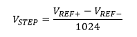
Step size is an analog voltage per unit of the ADC resolution.
For VREF+ = +5 V (VDD) and the VREF- = 0 V (VSS), we get the step size of
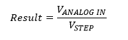
For example if the ADC result equal to 512, the voltage is,
Similarly, we get find the digital result equivalent to the analog input voltage,
In this example, I use a POT to adjust the analog input voltage varies from 0 to +5 V. To find the voltage we can use the equations listed above. But we can use another short form as,
In the C program, we must use the floating point to measure the analog voltage.
Schematic diagram. RB0 is AN12 analog input, measuring the input voltage
from 0 to +5 V. PORTC and PORTD display the measuring voltage with
one floating point.
The C source code:
#include<xc.h>
// PIC16F887 Configuration Bit Settings
// CONFIG1
#pragma config FOSC = XT
#pragma config WDTE = OFF
#pragma config PWRTE = OFF
#pragma config MCLRE = ON
#pragma config CP = OFF
#pragma config CPD = OFF
#pragma config BOREN = ON
#pragma config IESO = ON
#pragma config FCMEN = ON
#pragma config LVP = ON
// CONFIG2
#pragma config BOR4V = BOR40V
#pragma config WRT = OFF
/*_XTAL_FREQ use for __delay*/
#define _XTAL_FREQ 4000000

void driveDisplays(unsigned int analogRead){
 unsigned char ssd[16]={0x3F,0x06,0x5B,0x4F,0x66,0x6D,0x7D,
 0x07,0x7F,0x6F,0x77,0x7C,0x39,0x5E,0x79,0x71};
 float voltage;
 int _voltage;
 /*Voltage Calculation*/
 voltage=5*((float)analogRead/1024);
 _voltage=voltage*10;

 /*Decimal Place*/
 PORTD=0x00;
 PORTC=ssd[_voltage/10]|0x80;
 PORTD=0x01;
 __delay_ms(10);
 /*Floating point*/
 PORTD=0x00;
 PORTC=ssd[_voltage%10];
 PORTD=0x02;
 __delay_ms(10);
}
unsigned int readADC(void){
    GO=1;
    while(GO);
    __delay_ms(10);
    return (ADRESH<<8)+ADRESL;
}
void main(void){
    unsigned int adcResult;
    /*Analog and digital Port
     Configuration*/
    PORTB=0x00;
    PORTC=0x00;
    PORTD=0x00;
    TRISB=0x01;
    TRISC=0x00;
    TRISD=0x00;
    /*Result is right justify*/
    ADFM=1;
    /*By default is analog,
     but again set it to analog*/
    ANS12=1;
    /*Select FRC Clock of ADC module*/
    ADCON0bits.ADCS=0x03;
    /*Turn on ADC Module*/
    ADON=1;
    /*Select AN12 RB0*/
    ADCON0bits.CHS=0b1100;
    /*initiate a conversion*/
    GO=1;
    /*Wait until GO=0 "done"*/
    while(GO);
    while(1){
        adcResult=readADC();
        driveDisplays(adcResult);
        __delay_ms(20);
    }
}
Simulation screen shot. The measuring voltage displays 3.9 V DC.
An analog to digital converter (ADC) module converts an analog voltage to a digital binary equivalence value. In PIC16F887 the built-in ADC module use a successive approximation type. I has up to 14 analog channels with reference voltage selection. The ADC resolution is 10-bit, made up of two distinct 8-bit registers.
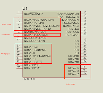
Some pins of PortA and PortB could be used for analog inputs.
Analog input pins of PIC16F887
There are two option of ADC clocks, MCU clock and the ADC built-in RC oscillator (FRC). The FRC gives a frequency of 500 kHz maximum. Using the MCU clock with the maximum clocking frequency, the ADC could complete the conversion time at 100 nano seconds.
A simplified scheme of ADC module in PIC16F887. An original detailed block diagram could be found in PIC16F887 datasheet.
ADC module takes up to 12 cycles to complete the conversion to make the 10-bit result ready. Since the 10-bit result consists of two 8-bit registers. It could be arranged in two margins, left or right.
Up on the completion, an interrupt flag relates to ADC is set. With this advantage, we can use interrupt routine to process the analog to digital conversion.
There are some registers to work with ADC module:
Input output port register (PORTx),
Port direction register (TRISx),
ANSEL and ANSELH registers,
ADCON0 and ADCON1 register,
related interrupt registers,
ADC result registers.
Some registers listed above have already discussed in previous posts. So we are listing some not-ready-listed registers.
This register set the analog inputs pins of some of PortA and PortE. Setting any bit to '1', assigning the corresponding pin to analog input. By default they are '1'.
ANSELH controls the analog input pin at PortB. It has only 6 analog input pins while the remaining two are digital. By default, they are set to '1'.
This is the first register to control the operation of ADC module.
ADC Conversion Clock Select bits ADCS[1:0], is a two-bit clock selection for ADC. The clock source for ADC could fed from MCU clock with the 2, 8 and 32 clock division. Another clock source could fed from internal ADC oscillator with the maximum frequency of 500 kHz. Setting ADCS to 0x03, the ADC clock is fed from it's internal oscillator.
Analog Channel Select bits CHS[3:0], could select between the 14 analog input channels. These bits could select the reference capacitor for analog comparator and the 0.6 V fixed voltage reference.
ADC Conversion Status bits GO/nDone, initiate a start of conversion when it's set to '1'. It will clear to '0' when the conversion completed. We can also use this bit to check the status of the conversion.
ADC Enable bit ADON, turn on the ADC module when set to '1'. Otherwise it's turned off.
ADCON1 configures additional setting of the ADC operation.
ADC Conversion Result format Select bit ADFM, arranges the margin of the ADC conversion result. It effect the ADRESL and ADRESH register. When it's '0' (default) the result is right justified.
Negative voltage reference bit VCFG1, set the negative voltage reference for ADC. Setting it to '1', the negative voltage reference must supply to VREF- pin. By default, it's '0' and the negative voltage reference pin is internally wired to VSS of the MCU.
Positive voltage reference bit VCFG0, set the positive voltage reference for ADC. Setting it to '1', the positive voltage reference must supply to VREF+ pin. By default, it's '0' and the positive voltage reference pin is internally wired to VDD of the MCU.
The ADC Result High Register ADRESH, store the result of ADC conversion. In the picture above, it's assumed that the result format is right justified (ADFM=1).
ADRESL is a pair register with ADRESH. Joining them together to make a 10-bit ADC resolution. In this picture we assume that the result format is right justified (ADFM=1).
Programming the ADC in XC8
To access to the ADC module, we must setting up the ADC module and work with the conversion process.
To set up the ADC module:
set the related pin to input
By default those related pins are analog inputs. But we can do it optionally, by setting any bits of the ANSEL and ANSELH register. These two registers contain the analog and digital pins selection as listed above.
Select the ADC clock source by setting the ADCS bits of the ADCON0 register.
Since there are 14 analog channels. Only one active channel is selected for reading the analog voltage value. So we must select one channel by setting the 4-bit CHS bits of the ADCON0 register.
Turn on the ADC module by setting the ADON bit of the ADCON0 register to '1'.
Two resolution register ADRESL and ADRESH pair store the conversion result. We must set it to right or left justification as preferred by assigning the value to ADFM bit of the ADCON1 register.
Select the voltage reference by setting any value to the VCFG1 and VCFG0 bits of the ADCON1 register.
To start a conversion:
If we are not yet select the analog channel, do it with the CHS bits.
Wait for some period to make the capacitor properly work
Set the GO/nDone bit to '1' to start the conversion
Wait for the completion by checking the GO/nDone bit.
Get the result from ADRESH and ADRESL register pair.
Programming Example
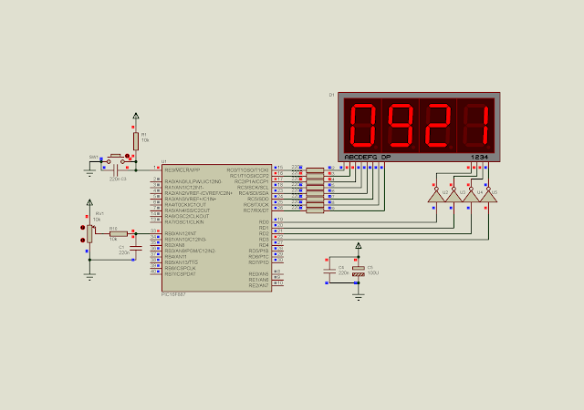
In this example I read an analog voltage value from AN12 input channel. The result is display in decimal (0 to 1023 for 10-bit value) on a multiplexed SSD.
The ADC clock is driven from its dedicated internal oscillator. The analog value is fed from a POT ranging from 0 to +5 V. The voltage references is internally wired to VSS and VDD of the MCU.
Schematic diagram. RB0 or AN12 is an analog input reading pin, reading an analog
value from the POT. The POT works with a passive low pass filter withe any
calculation. The result is displayed on a 4-digit multiplexed SSD ranging from
0 to 1023 in decimal value.
Source code is here.
#include<xc.h>
// PIC16F887 Configuration Bit Settings
// CONFIG1
#pragma config FOSC = XT
#pragma config WDTE = OFF
#pragma config PWRTE = OFF
#pragma config MCLRE = ON
#pragma config CP = OFF
#pragma config CPD = OFF
#pragma config BOREN = ON
#pragma config IESO = ON
#pragma config FCMEN = ON
#pragma config LVP = ON
// CONFIG2
#pragma config BOR4V = BOR40V
#pragma config WRT = OFF
/*_XTAL_FREQ use for __delay*/
#define _XTAL_FREQ 4000000

void driveDisplays(unsigned int cnt){
 unsigned char ssd[16]={0x3F,0x06,0x5B,0x4F,0x66,0x6D,0x7D,
 0x07,0x7F,0x6F,0x77,0x7C,0x39,0x5E,0x79,0x71};
 //Digit 4 1000's
 PORTD=0x00;
 PORTC=ssd[cnt/1000];
 PORTD=0x01;
 __delay_ms(10);
 //Digit 3 100's
 PORTD=0x00;
 PORTC=ssd[(cnt%1000)/100];
 PORTD=0x02;
 __delay_ms(10);
 //Digit 2 10's
 PORTD=0x00;
 PORTC=ssd[(cnt%100)/10];
 PORTD=0x04;
 __delay_ms(10);
 //Digit 1 1's
 PORTD=0x00;
 PORTC=ssd[cnt%10];
 PORTD=0x08;
 __delay_ms(10);
}
unsigned int readADC(void){
    GO=1;
    while(GO);
    __delay_ms(10);
    return (ADRESH<<8)+ADRESL;
}
void main(void){
    unsigned int adcResult;
    /*Analog and digital Port
     Configuration*/
    PORTB=0x00;
    PORTC=0x00;
    PORTD=0x00;
    TRISB=0x01;
    TRISC=0x00;
    TRISD=0x00;
    /*Result is right justify*/
    ADFM=1;
    /*By default is analog,
     but again set it to analog*/
    ANS12=1;
    /*Select FRC Clock of ADC module*/
    ADCON0bits.ADCS=0x03;
    /*Turn on ADC Module*/
    ADON=1;
    /*Select AN12 RB0*/
    ADCON0bits.CHS=0b1100;
    /*initiate a conversion*/
    GO=1;
    /*Wait until GO=0 "done"*/
    while(GO);
    while(1){
        adcResult=readADC();
        driveDisplays(adcResult);
    }
}
A simulation screen shot. The analog reading is 921 in decimal.