Introduction
In previous section we getting started with PIC16F877A with LED toggling on Port C. Now let move to its digital I/O port programming using XC8.
PIC16F877A has up to five digital I/O ports,
- Port A
- Port B
- Port C
- Port D
- and Port E
These ports are bi-directional I/O by program setting.
| PIC16F877A pin diagram |
Port C and Port D
These two ports are discussed first due to their pure digital I/O functions.
Port C
Port C locates at 07h in Special Function Register (SFR). Its data direction is controlled by TRISC register, locates at 87h in SFR.
| Registers associate with Port C |
Setting TRISC conveys Port C to input direction, accepting digital input data from outside world. Clearing TRISC to make Port C outputs its data via its output pins.
Port D
Port D locates at 08h in SFR. Its data direction is controlled by TRISD register, locates at 88h in SFR.
Setting TRISD conveys Port D to input direction, accepting digital data from outside world. Clearing this register to make Port D to outputs its data from its output pins.
| Registers associate with Port D |
Programming Example
A simple example shows how to read digital input Port C. Its digital data outputs on Port D.
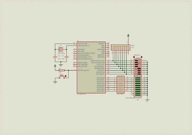
| Schematic Diagram |
Digital input made by a DIP switch with a resistor network. Digital output is an LED bar-graph.
/* * PIC16F877A digital I/O Programming in XC8 */ #include <xc.h> // PIC16F877A Configuration Bit Settings // CONFIG #pragma config FOSC = HS // Oscillator Selection bits (HS oscillator) #pragma config WDTE = OFF // Watchdog Timer Enable bit (WDT disabled) #pragma config PWRTE = OFF // Power-up Timer Enable bit (PWRT disabled) #pragma config BOREN = ON // Brown-out Reset Enable bit (BOR enabled) #pragma config LVP = OFF // Low-Voltage (Single-Supply) In-Circuit Serial Programming Enable bit (RB3 is digital I/O, HV on MCLR must be used for programming) #pragma config CPD = OFF // Data EEPROM Memory Code Protection bit (Data EEPROM code protection off) #pragma config WRT = OFF // Flash Program Memory Write Enable bits (Write protection off; all program memory may be written to by EECON control) #pragma config CP = OFF // Flash Program Memory Code Protection bit (Code protection off) void main(void){ /*Clear IO*/ PORTC=0x00; PORTD=0x00; /*Port C input*/ TRISC=0xFF; /*Port D output*/ TRISD=0x00; while(1){ PORTD=PORTC; for(int i=0;i<25;i++); } }
Click here to download zip file of this programming example.
Port B
Port B is an 8-bit wide bi-directional I/O. Its data direction is controlled by TRISD register. PORTB is its I/O register locate at 07h in SFR. TRISB locates at 87h.
Details
Setting TRISB allows Port B to accept digital input data, as it works in input data direction. By clearing it, digital data flows out via PORTB I/O register to output devices.
| Register associate with Port B |
RB0 of Port B can trigger an external interrupt but we don’t discuss it here. Port B has an internal weak pull up resistors. This feature is enabled by clearing RBPU bit of Option Register (OPTION_REG).
Programming Example
We will show how to configure Port B as digital input with its internal weak pull up resistors. Here Port D is a digital output port connecting to bar-graph LED.
Port B doesn’t need external resistors as it’s internally connected to VDD via its weak pull up resistors.
/* * PIC16F877A Port B digital I/O Programming in XC8 */ #include <xc.h> // PIC16F877A Configuration Bit Settings // CONFIG #pragma config FOSC = HS // Oscillator Selection bits (HS oscillator) #pragma config WDTE = OFF // Watchdog Timer Enable bit (WDT disabled) #pragma config PWRTE = OFF // Power-up Timer Enable bit (PWRT disabled) #pragma config BOREN = ON // Brown-out Reset Enable bit (BOR enabled) #pragma config LVP = OFF // Low-Voltage (Single-Supply) In-Circuit Serial Programming Enable bit (RB3 is digital I/O, HV on MCLR must be used for programming) #pragma config CPD = OFF // Data EEPROM Memory Code Protection bit (Data EEPROM code protection off) #pragma config WRT = OFF // Flash Program Memory Write Enable bits (Write protection off; all program memory may be written to by EECON control) #pragma config CP = OFF // Flash Program Memory Code Protection bit (Code protection off) void main(void){ /*Clear IO*/ PORTB=0x00; PORTD=0x00; /*Port B input*/ TRISB=0xFF; /*Turn on Weak Pull Up*/ OPTION_REGbits.nRBPU=0; /*Port C output*/ TRISD=0x00; while(1){ PORTD=PORTB; for(int i=0;i<25;i++); } }
Click here to download this example is zip format.
Port A
Port A is an 8-bit wide bi-directional I/O. Its data direction is controlled by TRISA register.
Details
PORTA is its I/O buffer locates at 05h in SFR. Its data direction control TRISA locates at 85h in SFR. Setting TRISA make this port as digital input, otherwise it becomes digital output.
| Registers associate with Port A |
Port A is multiplexed with Analog to Digital Converter (ADC) input. Setting Analog to Digital Control Register 1 (ADCON1) to 0x06 to analog input function, allowing this port work solely in digital I/O.
Programming Example
We make a simple port reading from Port A. Its digital value will be displayed on Port B.
Port A is usable only five bits. So I mask other two remaining MSB.
/* * PIC16F877A Port A Programming Example in XC8 */ #include <xc.h> // PIC16F877A Configuration Bit Settings // CONFIG #pragma config FOSC = HS // Oscillator Selection bits (HS oscillator) #pragma config WDTE = OFF // Watchdog Timer Enable bit (WDT disabled) #pragma config PWRTE = OFF // Power-up Timer Enable bit (PWRT disabled) #pragma config BOREN = ON // Brown-out Reset Enable bit (BOR enabled) #pragma config LVP = OFF // Low-Voltage (Single-Supply) In-Circuit Serial Programming Enable bit (RB3 is digital I/O, HV on MCLR must be used for programming) #pragma config CPD = OFF // Data EEPROM Memory Code Protection bit (Data EEPROM code protection off) #pragma config WRT = OFF // Flash Program Memory Write Enable bits (Write protection off; all program memory may be written to by EECON control) #pragma config CP = OFF // Flash Program Memory Code Protection bit (Code protection off) void main(void){ /*Clear IO*/ PORTB=0x00; PORTA=0x00; /*Port A input*/ TRISA=0xFF; /*Disable ADC input*/ ADCON1=0x06; /*Port B output*/ TRISB=0x00; while(1){ /*Read Port A input*/ PORTB=PORTA&0b00111111; /*A little delay*/ for(int i=0;i<10;i++); } }
Click here to download this example program.
No comments:
Post a Comment