PortE of dsPIC30F1010 is a 16-bit bi-directional I/O port. Within the 28-pin SOC package of this device, there are only six usable pins. They are not complex because there are not analog input function relate to this port.
Experiment on breadboard |
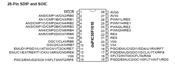
As it was shown in previous post, total pin numbers and its description is figured out below.
Pin diagram of dsPIC30F1010 |
In SFR of this controller, PORTE is an input register while LATE is an output register. To get digital input data PORTE register must be read. Writing digital data out, LATE must be modify. TRISE is data direction control register. Writing '1' to this register to make data register as digital input. Clearing this register to make data register as digital output.
dsPIC30F1010/2020 PORT REGISTER MAP |
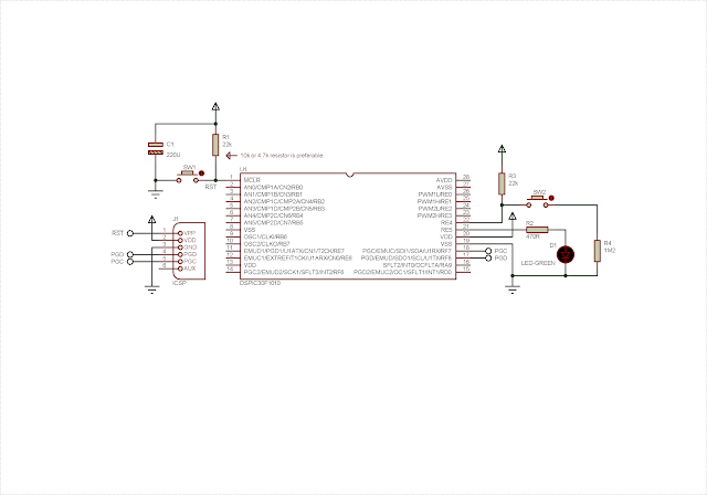
In this programming example I select RE4 as digital input, connecting to a button. RE5 connects an LED as a digital output.
Schematic diagram |
This system operates at 5VDC as it's supplied from PICKIT2 device programmer. Internal fast RC oscillator is used in this programming example to cut down component counts during prototyping on breadboard.
Pin 1 connects to reset circuit. Pressing SW1 to restart the system. Whenever SW2 is pressed and released, output LED D1 toggles its logic state.
Device's configuration setting is stored in "config.h" file of project directory.
Click here to download this example in zip file.


No comments:
Post a Comment