Learn To Write Code For 8051, Arduino, AVR, dsPIC, PIC, STM32 ARM Microcontroller, etc.
Coding Embedded Controller With C/C++.
Printed Circuit Board (PCB) Project For Electronics Hobbyists.
Port B of PIC18F1220 has an internal programmable weak pull up resistors. However it’s not individually select-able. These resistors have only one shared global switch locates in OPTION Register.
Pin diagram of PIC18F1220
Additionally, this port is multiplexed with ADC input. To configure it to a solely digital I/O, the user must check the ADCON1 register.
Interfacing and Programming
Using a simulator to simulate the circuit, the overall prototyping is fast and effective. It reduces cost, time and physical hardware defect.
Hardware Interfacing
PIC18F1220 microcontroller accept digital input on lower nibble of Port B. Its higher nibble connects to LED representing the digital input on lower nibble.
Schematic Diagram
Programming
At setting up section of C main program, programmer need to clear port I/O, disabling analog input function, setting up port direction, and turning on Port B weak pull up resistors.
C
/*
* PIC18F1220 Weak Pull Up Resistor
* And Disabling Analog Input on Port B
*/
#include <xc.h>
#include "config.h"
voidmain(void){
/*Clear Port B IO*/
PORTB=0x00;
LATB=0x00;
/*Disable Analog Input Function*/
ADCON1=0x70;
/*RB0...3 digital input*/
TRISB=0x0F;
/*Turn on Weak Pull Up*/
nRBPU=0;
while(1){
PORTB<<=4;
}
}
PIC18F1220 configuration bits setting is very long that programmer doesn’t want to put inside C main file.
#pragma config MCLRE = ON // MCLR Pin Enable bit (MCLR pin enabled, RA5 input pin disabled)
// CONFIG4L
#pragma config STVR = ON // Stack Full/Underflow Reset Enable bit (Stack full/underflow will cause Reset)
#pragma config LVP = OFF // Low-Voltage ICSP Enable bit (Low-Voltage ICSP disabled)
// CONFIG5L
#pragma config CP0 = OFF // Code Protection bit (Block 0 (00200-0007FFh) not code-protected)
#pragma config CP1 = OFF // Code Protection bit (Block 1 (000800-000FFFh) not code-protected)
// CONFIG5H
#pragma config CPB = OFF // Boot Block Code Protection bit (Boot Block (000000-0001FFh) not code-protected)
#pragma config CPD = OFF // Data EEPROM Code Protection bit (Data EEPROM not code-protected)
// CONFIG6L
#pragma config WRT0 = OFF // Write Protection bit (Block 0 (00200-0007FFh) not write-protected)
#pragma config WRT1 = OFF // Write Protection bit (Block 1 (000800-000FFFh) not write-protected)
// CONFIG6H
#pragma config WRTC = OFF // Configuration Register Write Protection bit (Configuration registers (300000-3000FFh) not write-protected)
#pragma config WRTB = OFF // Boot Block Write Protection bit (Boot Block (000000-0001FFh) not write-protected)
#pragma config WRTD = OFF // Data EEPROM Write Protection bit (Data EEPROM not write-protected)
// CONFIG7L
#pragma config EBTR0 = OFF // Table Read Protection bit (Block 0 (00200-0007FFh) not protected from table reads executed in other blocks)
#pragma config EBTR1 = OFF // Table Read Protection bit (Block 1 (000800-000FFFh) not protected from table reads executed in other blocks)
// CONFIG7H
#pragma config EBTRB = OFF // Boot Block Table Read Protection bit (Boot Block (000000-0001FFh) not protected from table reads executed in other blocks)
PIC18F1220 is an 8-bit Harvard architecture microcontroller. Its instruction is 8-bit wide. Its essential features are list below.
PIC18F1220/PIC18F1320 Summary
Only the features of PIC18F1220 we target.
PIC18F1220 device feature
A used PIC18F1220 in 18-pin DIP package
Memory
It has 4KBytes in program (Flash) memory. Due to its 16-bit wide instruction length, maximum number of instruction line is 2048 lines (16×2048). Its scratch pad Static RAM (SRAM) is 256 bytes. Non-volatile auxiliary storage EEPROM is 256bytes, keeping data persistent even the controller is power off.
Program counter is 21-bit in length (address up to 2Mbyte program memory). Reset vector locates at 0x0000. Unlike Mid-range PICMicro PIC18F1220 reset vectors locate at 0x0008 and 0x0018.
Digital I/O Port
This 18-pin in DIP package device has up to 16 digital I/O, regardless of other multiplexing functions.
Pin Diagram of PIC18F1220 in DIP package
Disabling reset pin, it can be configured as a digital input pin. User can configure RA6 and RA7 as digital I/O as long as it’s driven from internal RC oscillator. Port A and Port B are 8-bit wide.
There are three external interrupt sources relate to digital I/O. Each I/O source/sink current up to 25mA/25mA.
Analog Inputs
Analog to Digital Converter (ADC) inside this device is 10-bit in resolution. It has 7 input channel that multiplexed with digital I/O pins. These analog input pins range from RA0 to RA6. ADC must be properly configured in software.
Analog Outputs
It has an analog output – Pulse Width Modulation (PWM) inside its ECCP module. Requirements for PWM usage is its timer. PWM is useful for driving analog output device – electric motor, light dimming, DC/DC converter, etc.
Timers
Timer is an essential part of microcontroller. PIC18F1220 has up to 4 timers,
Timer0 – 8-bit
Timer1 – 16-bit
Timer2 – 16-bit
Timer3 – 16-bit
They are useful in creating precise timing delay, pulse counting, pulse measurement, waveform generation, and PWM output.
Communications
Enhanced Addressable USART is commonly communicate to host PC, and other USART devices – GSM module, bluetooth, etc. In PIC18F1220 it has many configurations.
There’s a pair of Serial Peripheral Interface (SPI) and Inter-integrated Circuit (I2C) in its SSP module.
Others
It has other features that we will not list their details here. They are,
Reset and its programmable brown out reset
Low voltage detect
Start up delay
Device operates up to 40MHz using its High Speed Phase Lock Loop (PLL).
Programming and Development Tools
Popular programming tools are high level programming/compiler. Embedded C is a first choice for most of small microcontroller nowadays.
C Compilers
There are some well known C compilers for this device:
Mikroelectronika MikroC
Custom Computer Service (CCS) PICC
MPLABX XC8
MPLABX XC8 developed by Microchip Technology. It has a free version with no code optimization and technical support. However its free version is suitable for students and hobbyists at no cost.
Development Tools
This low pin counts device is easily prototype on breadboard. However it will require more times and many types of error.
Using a simulator could save prototyping time and spending on components. It’s safe without burning components even it’s wrong wiring.
I prefer Proteus VSM for a decade now. It’s a paid software but I use it b sharing with my development team.
Programming with MPLABX XC8
MPLABX Integrated Development Environment (IDE) is a powerful software. Programmer can write codes and debug in software and hardware. Currently MPLABX version 5.40 is the latest version.
XC8 is a compiler that plugged into this software targeting 8-bit PIC micro-controllers. XC8 2.1 is currently the latest version.
Getting Startedwith Coding
Blinking LED on microcontroller port is an easiest starting up with embedded C programming. This introductory programming toggles Port B of PIC18F1220 on for 0.5 second and off for 1 second.
I don’t show project setting up in MPLABX XC8 due to repetition. To get started with this tool chain click here.
An electronics digital clock usually equipped with a Real Time Clock (RTC) IC – for example DS3231 RTC. However we can build a non-complex one’s using internal timer of a microcontroller. This feature doesn’t have time keeping as RTC chip. It lost all its previous timing when it’s powered off.
A commercial sample of DS3231 RTC module from Ali Express
Digital Clock made from Timer0
Timer0 module creates a precise timing when it’s running in timer mode. Timing tick period is configurable by user. A a simple programming example we start with showing timing data on a multiplexing display.
Hardware Preparation
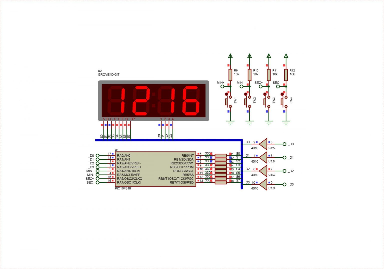
Main controller powered by PIC16F818 microcontroller. It’s suitable for this simple project. Display is assumed to be a dedicated digital clock display in multiplexing type. It’s common anode type as there’s no other option.
Schematic diagram
We don’t use external reset on RA5 pin. Higher nibble of Port A is reserved for digital inputs. These four inputs are minute and second adjustment. Controller clocks from its internal 8MHz oscillator.
Program Preparation
Blueprint of this digital clock project is Timer0 interrupt. Timer0 clock source is internal microcontroller clock with 1:2 prescaler. Timer0 interrupt creates timing tick of 100us. Each time the interrupt occurs Timer0 register is preloaded with 100 to get this timing interval.
Display
Multiplexing display is activated for every 5ms for each digit. A counting register schedule this task. It runs from 0 to 20ms before it rolls back to 0.
Buttons
Four input buttons are,
Increasing minute on RA4
Decreasing minute on RA5
Increasing second on RA6
Increasing second on RA7
Each button pressing will be accept by controller after 200ms. This 200ms timer tick create by buttonTime counting variable. Whenever any button is pressed time adjustment is made, and this time counting variable is reset to 0.
Timer0 Interrupt
ISR of PIC16F818 keeps track of Timer0 overflow interrupt. Each time interrupt occurs Timer0 Register (TMR0) preload with value of 100 to gain a 100us timer tick.
PIC16F818 C configuration settings store in “pic16f818Config.h” file.
// PIC16F818 Configuration Bit Settings // CONFIG #pragma config FOSC = INTOSCIO // Oscillator Selection bits (INTRC oscillator; port I/O function on both RA6/OSC2/CLKO pin and RA7/OSC1/CLKI pin) #pragma config WDTE = OFF // Watchdog Timer Enable bit (WDT disabled) #pragma config PWRTE = OFF // Power-up Timer Enable bit (PWRT disabled) #pragma config MCLRE = OFF // RA5/MCLR/VPP Pin Function Select bit (RA5/MCLR/VPP pin function is MCLR) #pragma config BOREN = ON // Brown-out Reset Enable bit (BOR enabled) #pragma config LVP = OFF // Low-Voltage Programming Enable bit (RB3/PGM pin has digital I/O function, HV on MCLR must be used for programming) #pragma config CPD = OFF // Data EE Memory Code Protection bit (Code protection off) #pragma config WRT = OFF // Flash Program Memory Write Enable bits (Write protection off) #pragma config CCPMX = RB2 // CCP1 Pin Selection bit (CCP1 function on RB2) #pragma config CP = OFF // Flash Program Memory Code Protection bit (Code protection off)
Click here to download source file. Its statistic shown below.