Learn To Write Code For 8051, Arduino, AVR, dsPIC, PIC, STM32 ARM Microcontroller, etc.
Coding Embedded Controller With C/C++.
Printed Circuit Board (PCB) Project For Electronics Hobbyists.
The LM35 is an analog temperature sensor with only three pins, positive supply voltage, ground and analog temperature output voltage. It could convert the temperature between -55 to 150 degree Celsius.
LM35DZ in TO-92 Package
Supply voltage ranges from 4 to 30 V. It’s temperature accuracy is about 0.25 degree Celsius. DOUT is the analog temperature output. The equivalence temperature is 10 mV per degree Celsius.
Typical connection diagram
PIC Programming And Interfacing
I use the ADC module of PIC16F819 to read the analog temperature value, fed into RA0.
In the positive temperature condition, LM35 creates a positive output voltage. Similarly, it creates a negative voltage output value in the below-zero temperature condition. The main problem is to make PIC16F819 able to read negative voltage value.
PIC16F819 has two voltage reference pins,
VREF+ at RA3
VREF- at RA2
But by default the voltage reference is internally connected to +5 V and GND. Anyway, I use external voltage references for the ADC. VREF+ connects to +2.5 V and VREF- connects to -2.5 V. The total reference voltage still stays at 5 V.
PIC16F819 has an internal RC oscillator, clocks up to 8 MHz. I decided to use this internal clock due to extra components placement and circuit designing add-on.
A character LCD displays connects to PORTB, displays the temperature data. It works in 4-bit mode.
Schematic Diagram
To create a -2.5/+2.5 V negative voltage pair, I use two 2.5 V zener diode pair as shown in the schematic diagram.
#include<16F819.h>
#device adc=10
#fuses INTRC_IO,NOWDT
#use delay(clock=8M)
#define LCD_ENABLE_PIN PIN_B2
#define LCD_RS_PIN PIN_B0
#define LCD_RW_PIN PIN_B1
#define LCD_DATA4 PIN_B4
#define LCD_DATA5 PIN_B5
#define LCD_DATA6 PIN_B6
#define LCD_DATA7 PIN_B7
#include<lcd.c>
voidmain(void){
char degree=223;
int16 adc;
float voltage;
setup_oscillator(OSC_8MHz);
output_A(0x00);
set_tris_A(0xFF);
setup_adc(ADC_CLOCK_INTERNAL );
set_adc_channel( 0 );
setup_adc_ports(AN0_VREF_VREF);
lcd_init();
lcd_gotoxy(1,1);
printf(LCD_PUTC,"Temperature:");
while(1){
adc=read_adc(ADC_START_AND_READ);
voltage=(adc*5.0)/1024;
voltage=voltage-2.5;
voltage*=100;
lcd_gotoxy(1,2);
printf(LCD_PUTC,"%0.2f %cC",voltage,degree);
}
}
This program consumes 78 % of program memory, and 16 % of device’s RAM.
Analog-to-Digital Converter (ADC) operates with analog signal input to microcontroller. Input signal from any device is converted to analog voltage before it’s fed to analog input pin.
Typical reference voltage of ADC is 5V. Maximum direct input voltage to analog input channel must not exceed +5V. For a 10-bit resolution ADC the step voltage is 0.048V.
In this example the controller is programmed to read and show input voltage to ADC input channel 0 – AN0 of PIC16F818. The result will show on a single common anode 7-Segments display.
Programming in MPLABX XC8
There are some additional codes over previous post that convert ADC result to analog voltage, and displaying. A display is one inch in digit size.
One inch red common anode seven-segments display
Circuit Design
System runs without external crystal oscillator as it comes with internal oscillator with maximum 8MHz frequency.
Schematic Design
AN0 reads input voltage while Port B display the result. Input voltage is varied due to the adjustment of RV1 POT.
Programming
Main program loop keeps track of ADC reading and result updating. Most of source code here is often seen in some previous posts relate to PIC16F818 ADC programming in MPLABX XC8.
/* * PIC16F818 Analog Voltage Reading */ #include <xc.h> // PIC16F818 Configuration Bit Settings #pragma config FOSC = INTOSCIO // Oscillator Selection bits (INTRC oscillator; port I/O function on both RA6/OSC2/CLKO pin and RA7/OSC1/CLKI pin) #pragma config WDTE = OFF // Watchdog Timer Enable bit (WDT disabled) #pragma config PWRTE = OFF // Power-up Timer Enable bit (PWRT disabled) #pragma config MCLRE = ON // RA5/MCLR/VPP Pin Function Select bit (RA5/MCLR/VPP pin function is MCLR) #pragma config BOREN = ON // Brown-out Reset Enable bit (BOR enabled) #pragma config LVP = OFF // Low-Voltage Programming Enable bit (RB3/PGM pin has digital I/O function, HV on MCLR must be used for programming) #pragma config CPD = OFF // Data EE Memory Code Protection bit (Code protection off) #pragma config WRT = OFF // Flash Program Memory Write Enable bits (Write protection off) #pragma config CCPMX = RB2 // CCP1 Pin Selection bit (CCP1 function on RB2) #pragma config CP = OFF // Flash Program Memory Code Protection bit (Code protection off) void readVoltage(void){ /*Seven-Segment output data*/ char displayAnode[10]={0xC0,0xF9,0xA4,0xB0,0x99,0x92,0x82,0xF8,0x80,0x90}; /*Start the conversion*/ ADCON0bits.GO_nDONE=1; /*When GO_nDONE is clear A/D conversion is completed*/ while(GO_nDONE); /*Wait for some microseconds*/ for(int i=0;i<1000;i++); /*Make a 10-bit A/D converter result*/ int _L=ADRESL; int _H=ADRESH; unsigned int adcResult=(_H<<8)+_L; /*convert to voltage with +0.1V offset*/ adcResult=(float)adcResult*5.1/1024; /*Show voltage reading*/ PORTB=displayAnode[adcResult]; } void main(void){ /*Select 8MHz internal oscillator*/ OSCCONbits.IRCF=0x07; /*Clear Port A*/ PORTA=0x00; /*Clear Port B*/ PORTB=0x00; /*RA0 analog input*/ TRISA=0x01; /*Port B digital output*/ TRISB=0x00; /*Select internal RC oscillator of A/D converter*/ ADCON0bits.ADCS=0x01; /*Select analog channel 0 - AN0*/ ADCON0bits.CHS=0x00; /*RA0-AN0 analog input, AVDD and AVSS voltage references*/ ADCON1bits.PCFG=14; /*Result is right justified*/ ADCON1bits.ADFM=1; /*Turn on A/D converter module*/ ADCON0bits.ADON=1; /*Main Program Loop*/ while(1){ readVoltage(); } }
Click hereto download zip file of this working example.
In previous article we have shown about A/D converter module of PIC16F818, and its programming example in MPLABX XC8. We are going to make more programming example using this analog input peripheral module inside this PIC device.
LED bar-graph is a popular LED display that show analog level status of any quantity – analog voltage, water level, and VU indicator. For example an bar-graph display indicating level of remaining energy of a smart phone power bank.
A simulation sample of this example
LED Bar-graph Programming Example With A/D Converter
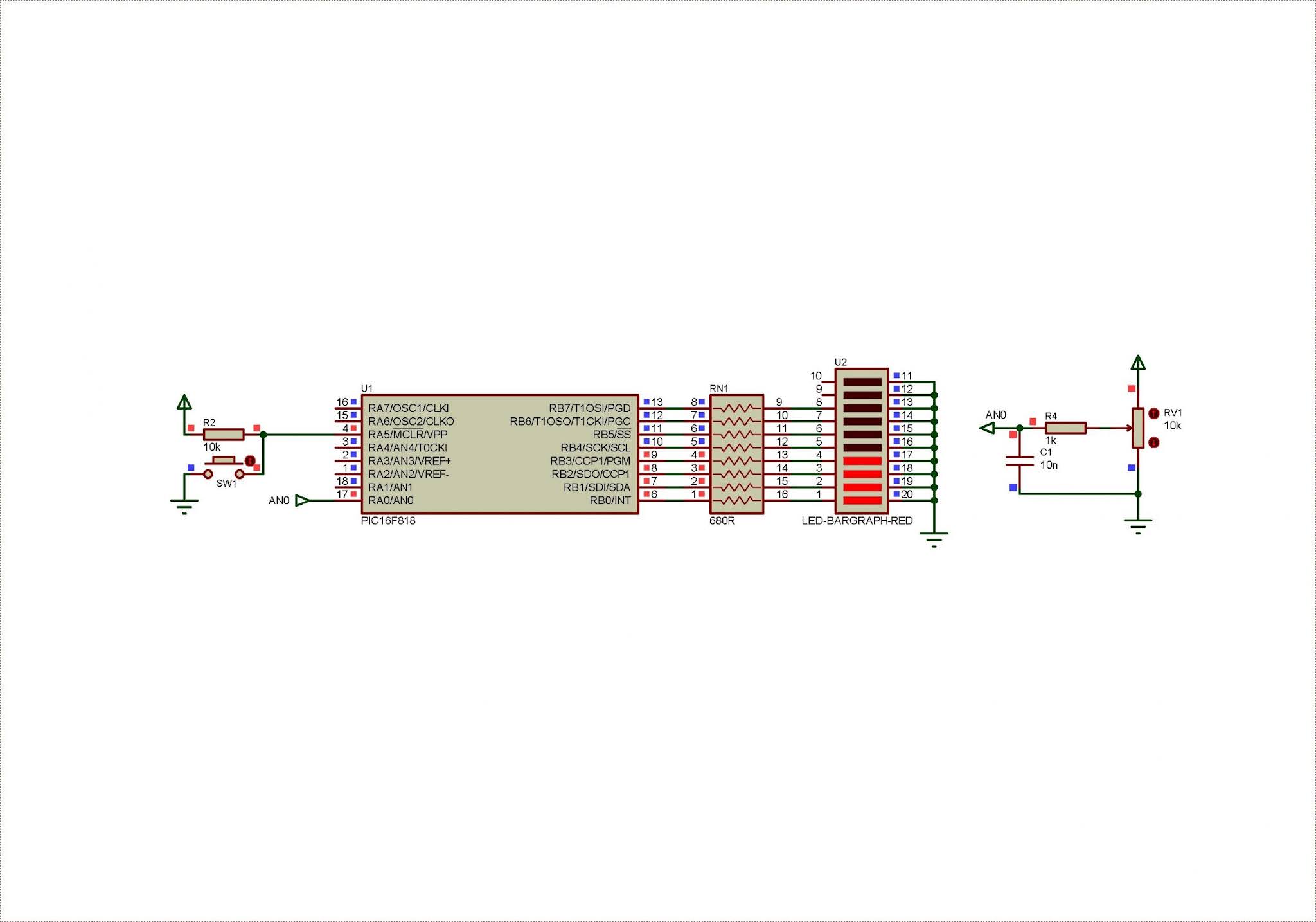
PIC microcontroller will be programmed to display bar-graph output with nine value – from null to its maximum display on. Analog input connects to RA0/AN0 while its analog representation will be displayed on Port B.
Circuit Design
Resistor network and LED bar-graph are more convenience in this programming example. They are packed in one package making an ease of circuit wiring on breadboard.
Circuit Diagram
This controller operates from its 8MHz internal oscillator due to economics issue and ease of design. An external reset on MCLR is needed as an aid of controller being stuck.
XC8 Programmingfor A/D Converter
Most of programming source code is similar to previous example. It excepts an additional lines of code that process bar-graph LED display. C program convert A/D converter 8-bit result pair to its 10-bit resolution.
An additional step converts this 1024 decimal value to 9 value range to fit 8-LED bar-graph display.
/* * PIC16F818 A/D Converter Example 2 * A/D reading bargraph display */ #include <xc.h> #include "pic16f818_config.h" /*Set oscillator to 8MHz*/ #define _XTAL_FREQ 8000000 void main(void){ /*LED Bar Graph Representation*/ char barGraph[9]={0,0b00000001,0b00000011,0b00000111,0b00001111, 0b00011111,0b00111111,0b01111111,0b11111111}; /*Select 8MHz internal oscillator*/ OSCCONbits.IRCF=0x07; /*Clear Port A*/ PORTA=0x00; /*Clear Port B*/ PORTB=0x00; /*RA0 analog input*/ TRISA=0x01; /*Port B digital output*/ TRISB=0x00; /*Select internal RC oscillator of A/D converter*/ ADCON0bits.ADCS=0x01; /*Select analog channel 0 - AN0*/ ADCON0bits.CHS=0x00; /*RA0-AN0 analog input, AVDD and AVSS voltage references*/ ADCON1bits.PCFG=14; /*Result is right justified*/ ADCON1bits.ADFM=1; /*Turn on A/D converter module*/ ADCON0bits.ADON=1; /*Main Program Loop*/ while(1){ /*Start the conversion*/ ADCON0bits.GO_nDONE=1; /*When GO_nDONE is clear A/D conversion is completed*/ while(GO_nDONE); /*Wait for some microseconds*/ for(int i=0;i<1000;i++); /*Make a 10-bit A/D converter result*/ int _L=ADRESL; int _H=ADRESH; unsigned int barValue=(_H<<8)+_L; /*Convert A/D result to 9 values*/ barValue=(float)barValue*9.0/1024; /*Display bargraph on Port B*/ PORTB = barGraph[barValue]; } }
Configuration bits keep in C header file “pic16f818_config.h” in the same project directory.
// PIC16F818 Configuration Bit Settings // CONFIG #pragma config FOSC = INTOSCIO // Oscillator Selection bits (INTRC oscillator; port I/O function on both RA6/OSC2/CLKO pin and RA7/OSC1/CLKI pin) #pragma config WDTE = OFF // Watchdog Timer Enable bit (WDT disabled) #pragma config PWRTE = OFF // Power-up Timer Enable bit (PWRT disabled) #pragma config MCLRE = ON // RA5/MCLR/VPP Pin Function Select bit (RA5/MCLR/VPP pin function is MCLR) #pragma config BOREN = ON // Brown-out Reset Enable bit (BOR enabled) #pragma config LVP = OFF // Low-Voltage Programming Enable bit (RB3/PGM pin has digital I/O function, HV on MCLR must be used for programming) #pragma config CPD = OFF // Data EE Memory Code Protection bit (Code protection off) #pragma config WRT = OFF // Flash Program Memory Write Enable bits (Write protection off) #pragma config CCPMX = RB2 // CCP1 Pin Selection bit (CCP1 function on RB2) #pragma config CP = OFF // Flash Program Memory Code Protection bit (Code protection off)
User can write these configuration codes within C main program.
Program Testing
This embedded controller program was primarily tested in software simulator.
Microcontroller simulation in Proteus 8
Click here to get zip file of this working example.