728x90

Saturday, May 30, 2020

Designing a positive and negative DC voltage meter using the 10-bit ADC module

The ADC module's resolution is up to 10-bit, yield an acceptable measuring accuracy with the voltage within 50 V DC.

In this example, I use this ADC module to measure a DC voltage within -25 V to +25 V. So the total voltage magnitude is 50 V.

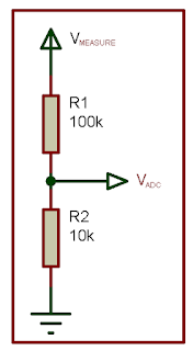
Since the maximum reference voltage is 5 V in magnitude. I use a voltage divider circuit to scale the input voltage to the lower 5 V.

Designing a positive negative voltage meter using the 10-bit ADC module

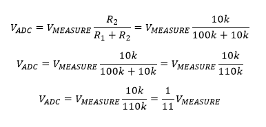
From the voltage divider:

Designing a positive negative voltage meter using the 10-bit ADC module

The V(ADC) is at 5 V maximum. V(MEASURE) could be 50 V in magnitude. So we divide the V(MEASURE) by 11.
But in the program simulation I don't use 11. I use 9 because it cause a lot of error. 
In the real hardware test, you can try 11.

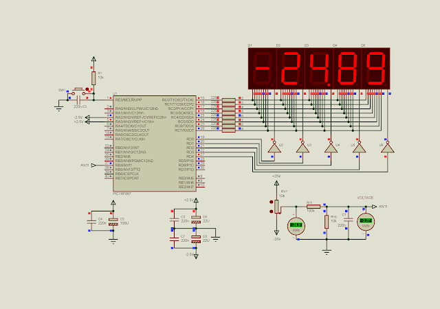
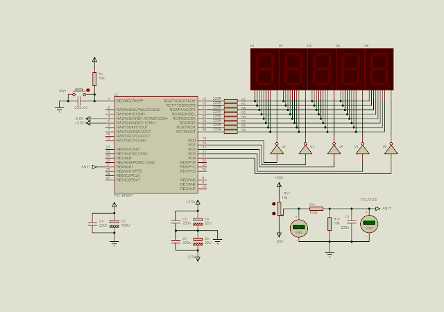
The voltmeter display the measuring voltage on a five-digit multiplexed SSD. The ADC reading is scheduled every one second due the timer 0 scheduling. The analog DC input voltage is fed from a -25 V and +25 V voltage terminals, giving a 50 V DC magnitude. 
Designing a positive and negative DC voltage meter using the 10-bit ADC module
Schematic diagram a digital two poles voltmeter. A POT used for adjusting the analog input
voltage, varies from -25 V to +25 V.

Source code:

#include<xc.h>
// PIC16F887 Configuration Bit Settings
// CONFIG1
#pragma config FOSC = XT
#pragma config WDTE = OFF
#pragma config PWRTE = OFF
#pragma config MCLRE = ON
#pragma config CP = OFF
#pragma config CPD = OFF
#pragma config BOREN = ON
#pragma config IESO = ON
#pragma config FCMEN = ON
#pragma config LVP = ON
// CONFIG2
#pragma config BOR4V = BOR40V
#pragma config WRT = OFF
/*_XTAL_FREQ use for __delay*/
#define _XTAL_FREQ 4000000

void driveDisplays(  int analogRead){
 unsigned char ssd[16]={0x3F,0x06,0x5B,0x4F,0x66,0x6D,0x7D,
 0x07,0x7F,0x6F,0x77,0x7C,0x39,0x5E,0x79,0x71};
 float voltage;
 int _voltage;
 /*Voltage Calculation total reference is
  +5V with centered ground*/
 voltage=((5.0*((float)(analogRead)/1024))-2.5)/9.1;
 //voltage/=11;
 _voltage=(int)(voltage*10000);
 /*Check negative voltage*/
 if(_voltage&0x8000){
     _voltage=-_voltage;
     PORTD=0x00;
 PORTC=0x40;
 PORTD=0x01;
 __delay_ms(10);
 }
 /*Decimal Place*/
 PORTD=0x00;
 PORTC=ssd[_voltage/1000];
 if(_voltage>=1000)
     PORTD=0x02;
 __delay_ms(10);
 /*Floating point*/
 PORTD=0x00;
 PORTC=ssd[(_voltage%1000)/100]|0x80;
 PORTD=0x04;
 __delay_ms(10);
 PORTD=0x00;
 PORTC=ssd[(_voltage%100)/10];
 PORTD=0x08;
 __delay_ms(10);
 PORTD=0x00;
 PORTC=ssd[_voltage%10];
 PORTD=0x10;
 __delay_ms(10);
}
int readADC(void){
    GO=1;
    while(GO);
    return (ADRESH<<8)+ADRESL;
}
void portInit(void){
    /*Analog and digital Port
     Configuration*/
    PORTB=0x00;
    PORTC=0x00;
    PORTD=0x00;
    /*RB4 for analog input*/
    TRISB4=1;
    TRISC=0x00;
    TRISD=0x00;
}
void adcInit(void){
    /*Select external Voltage reference
     +2.5V to -2.5V*/
    VCFG1=1;
    VCFG0=1;
    /*Result is right justify*/
    ADFM=1;
    /*By default is analog,
     but again set it to analog*/
    ANS11=1;
    /*Select FRC Clock of ADC module*/
    ADCON0bits.ADCS=0x03;
    /*Turn on ADC Module*/
    ADON=1;
    /*Select AN11 RB4*/
    ADCON0bits.CHS=0x0B;
    /*initiate a conversion*/
    GO=1;
    /*Wait until GO=0 "done"*/
    while(GO);
}
void timerInit(void){
     /*Select FOSC*/
    T0CS=0;
    /*Select timer 0 Prescaler*/
    PSA=0;
    /*Enable Timer 0 Overflow
     interrupt*/
    T0IE=1;
    /*Turn on Global interrupt
     Control*/
    GIE=1;
    /*Clear interrupt flage*/
    T0IF=0;
    /*Clear timer 0 register*/
    TMR0=0;
}
int adcResult;
int counter=0;
void main(void){
    portInit();
    adcInit();
    timerInit();
    
    while(1){
        driveDisplays(adcResult);
    }
}
void interrupt _ISR(void){
    if(T0IF){
        counter++;
        T0IF=0;
    }
    /* If it's one second*/
    if(counter>=15){
        adcResult=readADC();
        counter=0;
    }
}

Designing a positive and negative DC voltage meter using the 10-bit ADC module
A screen shot shows a positive voltage reading 24.84 V nearest to the positive terminal.

Designing a positive and negative DC voltage meter using the 10-bit ADC module
A screen shot shows a negative voltage reading -24.89 V nearest to the negative terminal.


Interfacing LM35 temperature sensor to the ADC module of PIC16F887

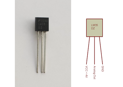
LM35 is an analog temperature sensor built in an integrated circuit. It could work in voltage range of -55 to +150 degree Celsius. It could be supply by a DC voltage between 4 to 30 V. It analog output is the temperature data. It is a linear output, 10 mV per degree Celsius.

Using the MCU ADC, it's easy to access rather using a complex protocol like one-wire or I2C bus.


Interfacing LM35 temperature sensor to the ADC module of PIC16F887
LM35 IC in TO-92 package and its pin out. 

To find the analog temperature data, we can find the digital ADC result per 10 mV. Or we can find the total voltage reading, multiplied by 100 to get the equivalent temperature in degree Celsius.

In this example, I use the ADC module to read the temperature data between -55 to 150 degree Celsius. The internal ADC module of PIC16F887 use -2.5 V to +2.5 V reference voltage, to make the device be able to read both negative and positive voltage.

I use timer 0 overflow interrupt to schedule the ADC reading for every one second.

The SSD is multiplexed with seven digits. Each digit turn on for every 5 milli seconds.


Interfacing LM35 temperature sensor to the ADC module of PIC16F887
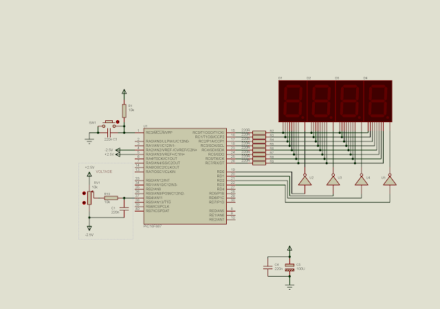
Schematic diagram. The LM35 connects to RB4/AN11 to convert the analog
temperature data. The display is multiplexed with seven digits SSD.

Source code's here:

#include<xc.h>
// PIC16F887 Configuration Bit Settings
// CONFIG1
#pragma config FOSC = XT
#pragma config WDTE = OFF
#pragma config PWRTE = OFF
#pragma config MCLRE = ON
#pragma config CP = OFF
#pragma config CPD = OFF
#pragma config BOREN = ON
#pragma config IESO = ON
#pragma config FCMEN = ON
#pragma config LVP = ON
// CONFIG2
#pragma config BOR4V = BOR40V
#pragma config WRT = OFF
/*_XTAL_FREQ use for __delay*/
#define _XTAL_FREQ 4000000
#define ssdRate 5
void driveDisplays(  int analogRead){
 unsigned char ssd[16]={0x3F,0x06,0x5B,0x4F,0x66,0x6D,0x7D,
 0x07,0x7F,0x6F,0x77,0x7C,0x39,0x5E,0x79,0x71};
 float voltage;
 int _voltage;
 /*Voltage Calculation total reference is
  +5V with centered ground*/
 voltage=(5*((float)(analogRead)/1024))-2.5;
 voltage*=10;
 /*Now _voltage becomes temperature,
  multiply it by 100 to convert it
  to the SSD data*/
 _voltage=(voltage*100);
 /*Check negative voltage*/
 if(_voltage&0x8000){
     _voltage=-_voltage;
     PORTD=0x00;
     PORTC=0x40;
     if((_voltage<1000)|(_voltage>-1000))
         PORTD=0x02;
     else
         PORTD=0x01;
     __delay_ms(ssdRate);
 }
 /*Decimal Place*/
 if((_voltage>=1000)|(_voltage<=-1000)){
 PORTD=0x00;
 PORTC=ssd[_voltage/1000];
 PORTD=0x02;
 __delay_ms(ssdRate);
 }
 PORTD=0x00;
 PORTC=ssd[(_voltage%1000)/100];
 if(_voltage>=100)
     PORTD=0x04;
 __delay_ms(ssdRate);
 /*Floating point*/
 PORTD=0x00;
 PORTC=ssd[(_voltage%100)/10]|0x80;
 PORTD=0x08;
 __delay_ms(ssdRate);
 PORTD=0x00;
 PORTC=ssd[_voltage%10];
 PORTD=0x10;
 __delay_ms(ssdRate);
 PORTD=0x00;
 PORTC=0x63;
 PORTD=0x20;
 __delay_ms(ssdRate);
 PORTD=0x00;
 PORTC=0x39;
 PORTD=0x40;
 __delay_ms(ssdRate);
}
int readADC(void){
    GO=1;
    while(GO);
    /*Return a 10-bit result*/
    return (ADRESH<<8)+ADRESL;
}
void portSetup(void){
    /*Analog and digital Port
     Configuration*/
    PORTB=0x00;
    PORTC=0x00;
    PORTD=0x00;
    /*RB4 for analog input*/
    TRISB4=1;
    TRISC=0x00;
    TRISD=0x00;
}
void timer0Setup(void){
    /*Select FOSC*/
    T0CS=0;
    /*Select timer 0 Prescaler*/
    PSA=0;
    /*Enable Timer 0 Overflow
     interrupt*/
    T0IE=1;
    /*Turn on Global interrupt
     Control*/
    GIE=1;
    /*Clear interrupt flage*/
    T0IF=0;
    /*Clear timer 0 register*/
    TMR0=0;
}
void adcSetup(void){
    /*Analog and digital Port
     Configuration*/
    PORTB=0x00;
    PORTC=0x00;
    PORTD=0x00;
    /*RB4 for analog input*/
    TRISB4=1;
    TRISC=0x00;
    TRISD=0x00;
    /*Select external Voltage reference
     +2.5V to -2.5V*/
    VCFG1=1;
    VCFG0=1;
    /*Result is right justify*/
    ADFM=1;
    /*By default is analog,
     but again set it to analog*/
    ANS11=1;
    /*Select FRC Clock of ADC module*/
    ADCON0bits.ADCS=0x03;
    /*Turn on ADC Module*/
    ADON=1;
    /*Select AN11 RB4*/
    ADCON0bits.CHS=0x0B;
    /*initiate a conversion*/
    GO=1;
    /*Wait until GO=0 "done"*/
    while(GO);
}
int adcResult;
int cnt=10;
void main(void){
    
    portSetup();
    adcSetup();
    timer0Setup();
    
    while(1){
        //adcResult=readADC();
        driveDisplays(adcResult);
    }
}
void interrupt _ISR(void){
    if(T0IF){
        cnt+=1;
        T0IF=0;
    }
    if(cnt>=15){
        adcResult=readADC();
        cnt=0;
    }
}


Interfacing LM35 temperature sensor to the ADC module of PIC16F887
A sample of simulation


Back to main tutorials page.


Friday, May 29, 2020

Working with ADC references voltage of PIC16F887

By default two references voltages of the ADC internally connected to VDD and VSS, supplying a +5 V reference voltage for the ADC module. We can change the reference voltage to any value in the total range of +5 V DC.

The VREF+ and VREF- pin could be programmed to externally connect to any voltage reference. By assigning the 'VCFG0' to '1' allows the VREF+ pin connect to external positive voltage. Similarly, by assigning the 'VCFG1' to '1' allows the VREF- pin connect to external negative voltage.

For this example, I connect the VREF+ pin to +2.5 V and the VREF- pin to -2.5 V. Hence, the total reference voltage for the ADC module is,

Working with ADC reference voltage of PIC16F887

The step voltage size is 0.00488 V. In this case the the lowest voltage of -2.5 V gives the ADC reading result 0. While the maximum voltage +2.5 V gives the ADC reading result 1023. The zero analog input voltage yields the ADC reading result to 512.


Working with ADC reference voltage of PIC16F887
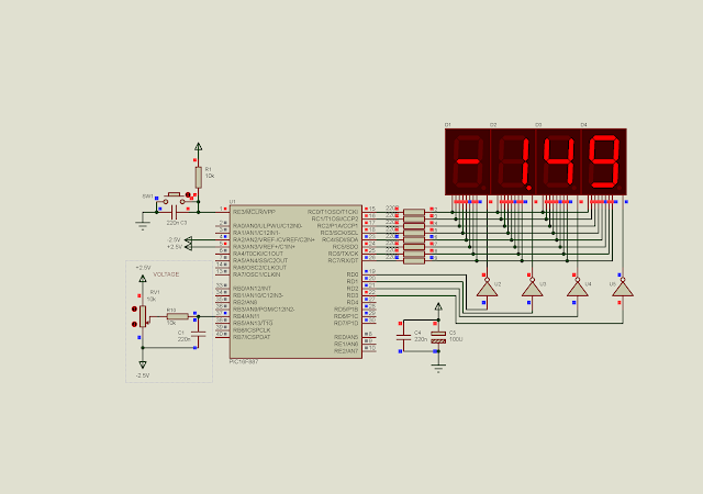
Schematic diagram. RA3/AN3 is used for positive voltage reference connects to +2.5 V.
RA2/AN2 is used for negative voltage reference connects to -2.5 V. The voltage reading displays
between -2.5 V to +2.5 V.

Source code:

#include<xc.h>
// PIC16F887 Configuration Bit Settings
// CONFIG1
#pragma config FOSC = XT
#pragma config WDTE = OFF
#pragma config PWRTE = OFF
#pragma config MCLRE = ON
#pragma config CP = OFF
#pragma config CPD = OFF
#pragma config BOREN = ON
#pragma config IESO = ON
#pragma config FCMEN = ON
#pragma config LVP = ON
// CONFIG2
#pragma config BOR4V = BOR40V
#pragma config WRT = OFF
/*_XTAL_FREQ use for __delay*/
#define _XTAL_FREQ 4000000

void driveDisplays(  int analogRead){
 unsigned char ssd[16]={0x3F,0x06,0x5B,0x4F,0x66,0x6D,0x7D,
 0x07,0x7F,0x6F,0x77,0x7C,0x39,0x5E,0x79,0x71};
 float voltage;
 int _voltage;
 /*Voltage Calculation total reference is
  +5V with centered ground*/
 voltage=(5*((float)(analogRead)/1024))-2.5;
 _voltage=(voltage*100);
 /*Check negative voltage*/
 if(_voltage&0x8000){
     _voltage=-_voltage;
     PORTD=0x00;
 PORTC=0x40;
 PORTD=0x01;
 __delay_ms(10);
 }
 /*Decimal Place*/
 PORTD=0x00;
 PORTC=ssd[_voltage/100]|0x80;
 PORTD=0x02;
 __delay_ms(10);
 /*Floating point*/
 PORTD=0x00;
 PORTC=ssd[(_voltage%100)/10];
 PORTD=0x04;
 __delay_ms(10);
 PORTD=0x00;
 PORTC=ssd[_voltage%10];
 PORTD=0x08;
 __delay_ms(10);
}
int readADC(void){
    GO=1;
    while(GO);
    __delay_ms(10);
    return (ADRESH<<8)+ADRESL;
}
void main(void){
      int adcResult;
    /*Analog and digital Port
     Configuration*/
    PORTB=0x00;
    PORTC=0x00;
    PORTD=0x00;
    /*RB4 for analog input*/
    TRISB4=1;
    TRISC=0x00;
    TRISD=0x00;
    /*Select external Voltage reference
     +2.5V to -2.5V*/
    VCFG1=1;
    VCFG0=1;
    /*Result is right justify*/
    ADFM=1;
    /*By default is analog,
     but again set it to analog*/
    ANS11=1;
    /*Select FRC Clock of ADC module*/
    ADCON0bits.ADCS=0x03;
    /*Turn on ADC Module*/
    ADON=1;
    /*Select AN11 RB4*/
    ADCON0bits.CHS=0x0B;
ADON=1;
    /*initiate a conversion*/
    GO=1;
    /*Wait until GO=0 "done"*/
    while(GO);
    while(1){
        adcResult=readADC();
        driveDisplays(adcResult);
        
    }
}

Working with ADC reference voltage of PIC16F887
The screen-shot shows the analog voltage input of -1.49 V. 

Back to main tutorials page.


Search This Blog