Overview
The PCF8574 is an 8-bit input/output (I/O) expander for the two-wire bidirectional bus (I2C), designed for 2.5V to 6V VCC operation.
The PCF8574 device provides general-purpose remote I/O expansion for most micro-controller
families by way of the I2C interface [serial clock (SCL), serial data (SDA)].
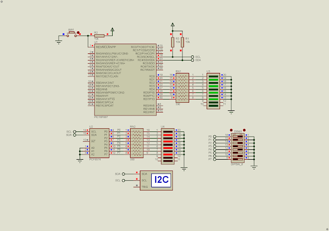 |
| Simulating Program |
The device features an 8-bit quasi-bidirectional I/O port (P0–P7), including latched outputs with high current drive capability for directly driving LEDs. Each quasi-bidirectional I/O can be used as an input or output without the use of a data-direction control signal. At power on, the I/Os are high. In this mode, only a current source to VCC is active.
This chip is suitable for,
- Telecom Shelters: Filter Units
- Servers
- Routers (Telecom Switching Equipment)
- Personal Computers
- Personal Electronics
- Industrial Automation
- Products with GPIO-Limited Processors
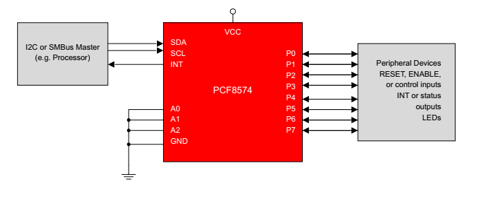 |
| PCF8574 Interfacing Diagram |
.jpg) |
| PCF8574AP DIP-16 |
We can event use this chip for a 4x4 matrix keypad, or driving an HD44780-base character LCD.
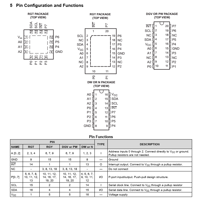 |
| Pin Configuration and Functions |
This device has various package types. A PDIP-16 or a SOIC-16 are common for most of electronics hobbyists.
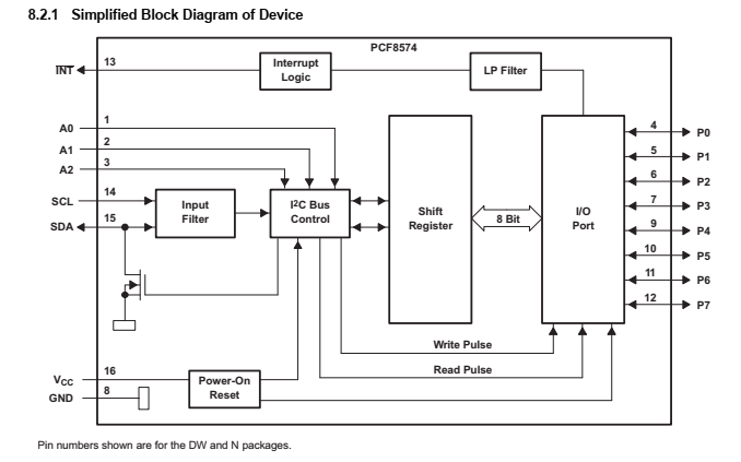 |
| Simplified Block Diagram of Device |
This device has an 8-bit customizable slave address with R/W bit.
 |
| PCF8574 Interface Definition |
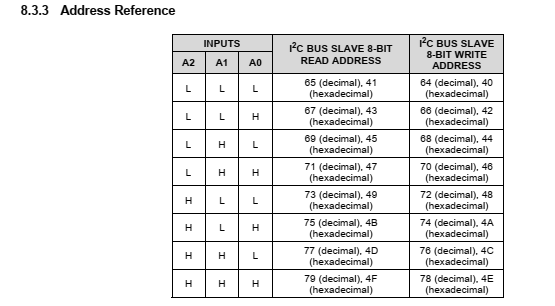 |
| Address Reference |
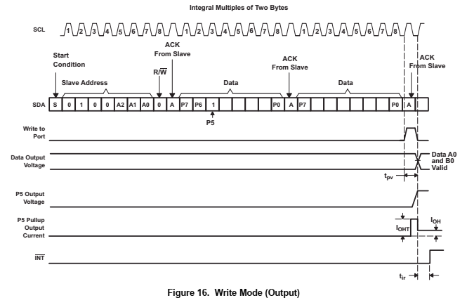 |
| PCF8574 Write Mode |
To read from this I2C slave device, the microprocessor need to write device read address (eg. 0x41), followed by I2C in read mode.
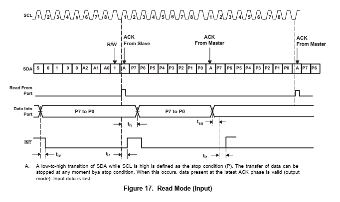 |
| PCF8574 Read Mode |
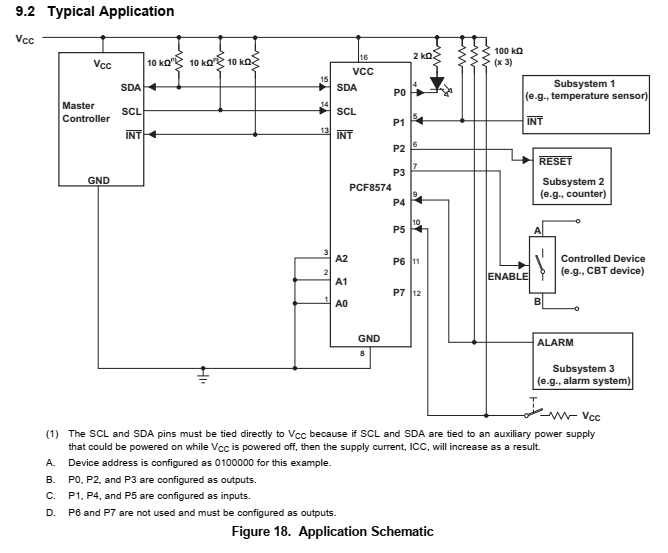 |
| PCF8574 Typical Application |
Interrupt Output (INT) pin is optional.
PIC16F887 MPLABX IDE and XC8 Programming
The PIC16F887 micro-controller has a high speed Inter Integrated Circuit (I2C) module that can operate in both master and slave mode.
In this example, I set up its I2C module to operate in master mode at 100kHz serial clock frequency. The program keeps reading input data from PCF8574 I/O port, its 8-bit content will show on PORTD of PIC16F887.
Since A2...A0 pins of PCF8574 are logic 0. So its device write address is 0x40, and 0x41 for device read address.
Click here to download its source file. See Also,
No comments:
Post a Comment