Microchip MCP492X SPI Digital To Analog Converter
MCP492X is a 12-bit digital to analog converter (DAC) with SPI interface. MCP4921 is a single output DAC while MCP4922 has two configurable DAC. This SPI DAC could clock up to 20 MHz. |
| A sample of this programming example |
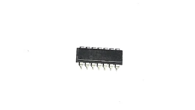
In this post I use MCP4922 I possess. I bought this chip from Futurlec on-line store a few years ago. It comes with an easy to prototype 14-bit DIP.
 |
| MCP4922 14-pin DIP Package |
 |
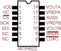
| MCP4922 14-pin DIP pin diagram |
These are the pins description of this IC:
- VDD is positive supply voltage for internal device working (2.7 V to 5.5 V).
- NC - No Connection
- CS - Chip Select Input
- SCK - Serial Clock Input
- SDI - Serial Data Input
- NC - No Connection
- NC - No Connection
- LDAC - is active low. It transfers DAC setting from serial latches to output latches.
- SHDN - Hardware shut down input
- VOUTB - DAC_B Output
- VREFB - DAC_B Voltage Input (AVSS To VDD)
- AVSS - Analog ground
- VREFA - DAC_A Voltage Input (AVSS to VDD)
- VOUTA - DAC_A Output
The data format transfers to this device is 16-bit wide. One upper nibble is the DAC configuration bits while the remaining 12-bit is the DAC output value. The output value to DAC is up 4096 maximum.
DAC output voltage - VOUT lists as follow:
Where,
- VREF is DAC voltage reference input. It could be DAC_A or DAC_B
- G is output voltage gain, 1X or 2X.
- DN is 12-bit DAC data input value
- 2^N is the DAC resolution. In this case, the resolution is 12-bit yield the decimal value to 2^12 = 4046
The 16-bit SPI data representation lists below.
 |
| MCP4922 Write Command Register |
Each bit functions as below.
- Bit 15 - A/B - Write '0' for DAC_A, otherwise DAC_B
- Bit 14 - BUF - Write '0' for Unbuffered, otherwise Buffered.
- Bit 13 - GA - Write '0' 1x Gain, otherwise 2x Gain.
- Bit 12 - SHDN - Write '0' to disable output buffer, otherwise enable the output buffer.
- Bit 11:0 - D11:D0 - 12-bit digital data DAC output ranges from 0 to 4095 (4096 in total).
Data transfer to this device is 16-bit, we need to send 8-bit twice with only on latching pulse.
 |
| Writing the command to MCP4922. External wiring is not include here. |
Interfacing And Programming With Atmel Studio 7 In C
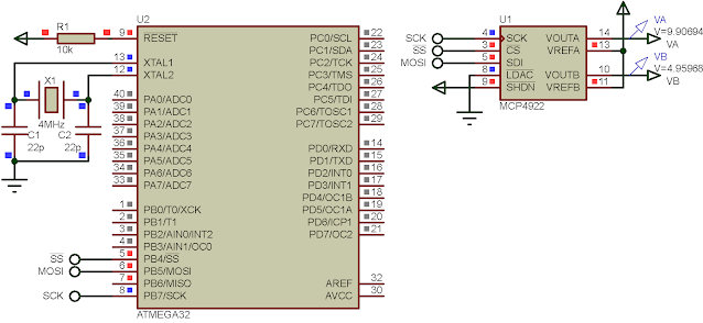
In this example, I use both output DAC. Both DAC outputs the maximum 12-bit value, 0xFFF or 4096. With 2X gain, DAC A generate the output voltage nearest to 10 V. Similarly, using 1X gain, DAC B generate output the voltage nearest to 5 V. The sample of this program lists below. The reference voltage for both DAC is 5 V.
 |
| A sample of this programming example |
C source code:
Schematic Diagram
 |
| Schematic Diagram for simulation |

Well done. Can you do this in a similar way with Arduino Uno? I am about to control a joystick of a wheelchair with Arduino and remote control. The joystick, however, requires 5 clear sine lines. That's why I got 3 DAC MCP4922 for it. But I can't do it, I don't know my way around that well. Do you have the time and inclination to realize something like that and publish it? You will also get a present from me.
ReplyDeletegreetings
Archie
Hi
DeleteHere I'm spending time to complete my work on AVR ATMega32 and PIC examples.
However Arduino requires more physical hardware and time consuming to prototype.
Thanks