- a timing delay
- a frequency generator
- or a user-defined PWM signal
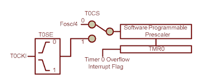
In counter mode, we could use it to count external input pulses fed to pin RA4/T0CKI. The counting result automatically stores in the TMR0 register of the SFR. TMR0 is used for both timer and counter mode.
Both timer and counter mode, have an 8-bit prescaler. This prescaler divide into two group, TMR0 prescaler and WDT prescaler. TMR0 prescaler ranges from 1:2 to 1:256. While WDT prescaler ranges from 1:1 to 1:128.
 |
| Timer 0 simplified block diagram |
Timer or counter 0 overflow could set an interrupt flag in the INTCON register. This flag is set when the TMR0 register rolls from 0xFF to 0x00.
These are some registers relate to timer/counter 0:
- OPTION_REG
- TMR0
- INTCON
Now let see the option register:
| BIT 7 | BIT 0 | ||||||
| nRBPU | INTEDG | T0CS | T0SE | PSA | PS2 | PS1 | PS0 |
This 8-bit register is high by default.
- The timer 0 clock source bit (T0CS) uses for selection between internal CPU clock source and external clock pulse fed to pin T0CKI. When '0' the Fosc/4 clock source fed the timer/counter.
- The timer 0 source edge select bit (T0SE) uses for select the edge of clock pulse fed to T0CKI pin. When '0' a low to high transition activate the counting.
- The prescaler assignment bit (PSA) select between two prescaler, timer 0 prescaler and the WDT one's.
- Prescaler rate select bit (PS[2:0]) set the rate of prescaler. These 3-bit wise selector set the prescaler from 1:1 to 1:256.
| PS[2:0] | TMR0 Prescaler | WDT Prescaler |
| 000 | 1:2 | 1:1 |
| 001 | 1:4 | 1:2 |
| 010 | 1:8 | 1:4 |
| 011 | 1:16 | 1:8 |
| 100 | 1:32 | 1:16 |
| 101 | 1:64 | 1:32 |
| 110 | 1:128 | 1:64 |
| 111 | 1:256 | 1:128 |
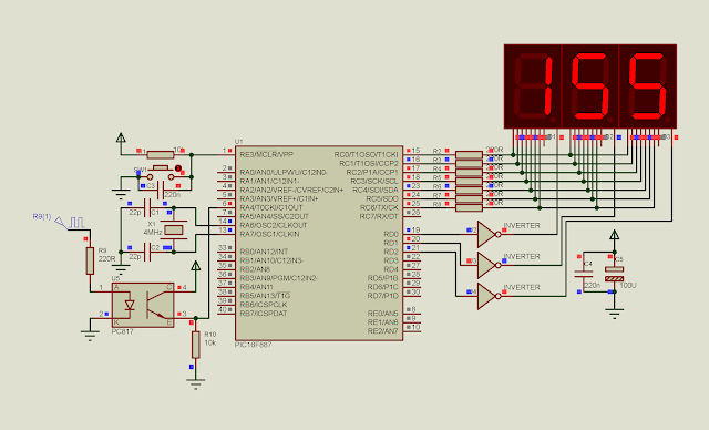
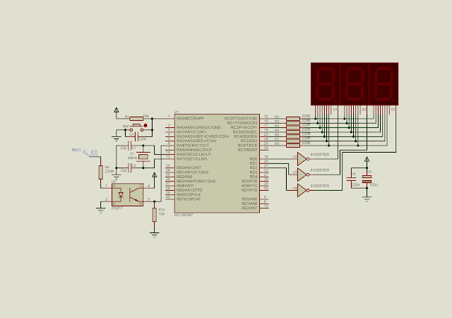
In the example below, I use T0CKI pin to count the external pulse from an external clock source. It has an application, for example a production counter at the output line in the factory.
Using the WDT prescaler, I set the prescaler rate to 1:1. So TMR0 will increase every rising edge of the T0CKI pin.
I use a three digits display to show the counts. It is 255 maximum before rolling back to 0. We can count the amount of pulse larger than this 8-bit TMR0 by using timer 0 overflow interrupt flag with some math calculations.
XC8 source code is here:
#include "xc.h"
// PIC16F887 Configuration Bit Settings
// CONFIG1
#pragma config FOSC = XT
#pragma config WDTE = OFF
#pragma config PWRTE = OFF
#pragma config MCLRE = ON
#pragma config CP = OFF
#pragma config CPD = OFF
#pragma config BOREN = ON
#pragma config IESO = ON
#pragma config FCMEN = ON
#pragma config LVP = OFF
// CONFIG2
#pragma config BOR4V = BOR40V
#pragma config WRT = OFF
/*_XTAL_FREQ use for __delay*/
#define _XTAL_FREQ 4000000
void displayCounter(void){
    unsigned char ssd[16]={0x3F,0x06,0x5B,0x4F,0x66,0x6D,0x7D,
        0x07,0x7F,0x6F,0x77,0x7C,0x39,0x5E,0x79,0x71};
    PORTD=0x00;
    PORTC=ssd[TMR0/100];
    RD0=1;
    __delay_ms(15);
    PORTD=0x00;
    PORTC=ssd[(TMR0%100)/10];
    RD1=1;
    __delay_ms(15);
    PORTD=0x00;
    PORTC=ssd[TMR0%10];
    RD2=1;
    __delay_ms(15);
}
void main(){
    //Port configuration
    PORTC=0x00;
    TRISC=0x80;
    PORTD=0x00;
    TRISD=0xF8;
    /*use rising edge transition*/
    T0SE=0;
    /*use 1:1 rate*/
    OPTION_REGbits.PS=0x00;
    TMR0=0;
    while(1){
        displayCounter();
    }
}
I took a simulation screen shot of this program.
 |
| Simulation screen shot. The content of TMR0 is 155 in decimal. |

No comments:
Post a Comment