Introduction
PIC18F1220 has two 8-bit digital I/O ports – Port A and Port B. They are bi-directional readable and writable. Their data directions are controlled by their TRIS registers.
Port A
Port A data direction is controlled by TRISA. Setting this registers allowing this port to accept input data, otherwise outputting digital data.
PORTA is considered as an input buffer. LATA is an output buffer. These two registers must be cleared before configuring its data direction.
 |
| Pin diagram of PIC18F1220 |
Port B
Port B data direction is controlled by TRISB. Setting this register allowing this port to accept input data, otherwise outputting digital data.
PORTB is considered as an input buffer. LATB is an output buffer. These two registers must be cleared before configuring its data direction.
Port B Programming Example
Since Port A and Port B are multiplexed with analog input function. I decided to select some pin of Port B that are solely digital I/O pin.
Schematic Diagram
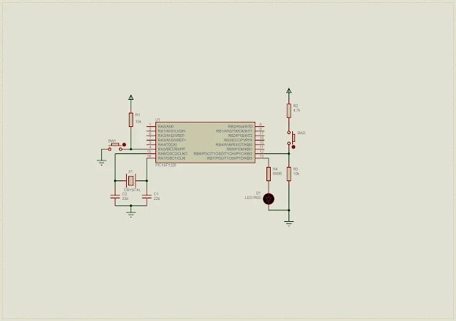
RB6 of Port B is selected as a digital input pin connecting to a push button. RB7 connects to an output LED. Whenever push button is pressed the controller toggle output LED.
 |
| Schematic Diagram |
External crystal oscillator has a frequency of 4MHz.
MPLABX XC8 Programming
This introductory tutorial is written in XC8 in MPLABX IDE. Overall program made of a dozen of lines.
Configuration bit of PIC18F1220 putted separately in “config.h” file.
Click here to download zip file of this programming example.
